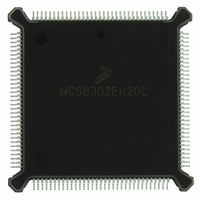
MC68302EH20C Freescale Semiconductor, MC68302EH20C Datasheet - Page 428

MC68302EH20C
Manufacturer Part Number
MC68302EH20C
Description
IC MPU MULTI-PROTOCOL 132-PQFP
Manufacturer
Freescale Semiconductor
Datasheets
1.MC68302AG20C.pdf
(4 pages)
2.MC68302AG20C.pdf
(2 pages)
3.MC68302AG20C.pdf
(13 pages)
4.MC68302EH20C.pdf
(481 pages)
Specifications of MC68302EH20C
Processor Type
M683xx 32-Bit
Speed
20MHz
Voltage
5V
Mounting Type
Surface Mount
Package / Case
132-MQFP, 132-PQFP
Family Name
M68000
Device Core
ColdFire
Device Core Size
32b
Frequency (max)
20MHz
Instruction Set Architecture
RISC
Supply Voltage 1 (typ)
5V
Operating Temp Range
0C to 70C
Operating Temperature Classification
Commercial
Mounting
Surface Mount
Pin Count
132
Package Type
PQFP
Lead Free Status / RoHS Status
Lead free / RoHS Compliant
Features
-
Lead Free Status / Rohs Status
Compliant
Available stocks
Company
Part Number
Manufacturer
Quantity
Price
Company:
Part Number:
MC68302EH20C
Manufacturer:
Freescale Semiconductor
Quantity:
10 000
Part Number:
MC68302EH20C
Manufacturer:
FREESCALE
Quantity:
20 000
Company:
Part Number:
MC68302EH20CB1
Manufacturer:
Freescale Semiconductor
Quantity:
10 000
Company:
Part Number:
MC68302EH20CR2
Manufacturer:
Freescale Semiconductor
Quantity:
10 000
- MC68302AG20C PDF datasheet
- MC68302AG20C PDF datasheet #2
- MC68302AG20C PDF datasheet #3
- MC68302EH20C PDF datasheet #4
- Current page: 428 of 481
- Download datasheet (2Mb)
SCC Programming Reference
E.1.1.2 PER SCC REGISTERS. Each of the three SCCs has a set of the following six reg-
isters. These registers configure the SCC and the protocol operation. Some parameters and
register bits are protocol independent. The HDLC functions have been given for those
parameters and bits that are protocol specific.
E.1.1.2.1 Serial Configuration Register (SCON). This 16-bit register is located at offset
$882 (SCC1), $892 (SCC2), and $8A2 (SCC3). The SCON register is used to select the
clock source and baud rate for the SCC.
WOMS—Wired-OR Mode Select
EXTC—External Clock Source
TCS—Transmit Clock Source
RCS—Receive Clock Source
CD10—CD0—Clock Divider
DIV4—SCC Clock Prescaler Divide by 4
E.1.1.2.2 SCC Mode Register (SCM). This 16-bit register is located at offset $884
(SCC1), $894 (SCC2), and $8A4 (SCC3). The SCM register configures the operation of the
SCC and defines HDLC specific parameters. Note that reserved bits in registers should be
written as zeros.
E-6
WOMS EXTC
15
Used to preset the 11-bit counter that is decremented at the prescaler output rate.
NOF3
FLG
0 = TXD driver operates normally.
1 = TXD driver functions as an open-drain output and may be wired together with other
0 = The internal main clock is the source for the baud rate generator.
1 = The external clock on the TIN1 pin is the source for the baud rate generator.
0 = Transmit clock source is the baud rate generator output.
1 = Transmit clock source is the clock signal on TCLK pin.
0 = Receive clock source is the baud rate generator output.
1 = Receive clock source is the clock signal on RCLK pin.
0 = Divide-by-1 prescaler.
1 = Divide-by-4 prescaler.
15
7
14
TXD pins.
TCS
13
NOF2
ENC
14
6
RCS
12
CD10
11
DIAG1
NOF1
13
5
CD9
10
MC68360 USER’S MANUAL
CD8
9
DIAG0
NOF0
12
4
CD7
8
CD6
7
ENR
C32
11
3
CD5
6
CD4
5
FSE
ENT
10
2
CD3
4
CD2
3
MODE1
—
9
1
CD1
2
MOTOROLA
CD0
1
M0DE0
RTE
8
0
DIV4
0
Related parts for MC68302EH20C
Image
Part Number
Description
Manufacturer
Datasheet
Request
R
Part Number:
Description:
Manufacturer:
Freescale Semiconductor, Inc
Datasheet:

Part Number:
Description:
MC68302 Configuring the Chip Selects on the MC68302
Manufacturer:
Motorola / Freescale Semiconductor

Part Number:
Description:
MC68302 Design Concept - Expanding Interrupts on the MC68302
Manufacturer:
Motorola / Freescale Semiconductor

Part Number:
Description:
MC68302 MC68302 Adapting a WAN Controller to a LAN Environment
Manufacturer:
Motorola / Freescale Semiconductor

Part Number:
Description:
MC68302 EKB Applications - Power Measurements on the MC68302
Manufacturer:
Motorola / Freescale Semiconductor

Part Number:
Description:
MC68302 Interfacing the MC68020 to a Slave MC68302
Manufacturer:
Motorola / Freescale Semiconductor

Part Number:
Description:
MC68302 MC68302 Software Performance
Manufacturer:
Motorola / Freescale Semiconductor

Part Number:
Description:
MC68302 Evaluating EDX on the ADS302
Manufacturer:
Motorola / Freescale Semiconductor

Part Number:
Description:
MC68302 Design Advisory #1 - MC68SC302 Passive ISDN Protocol Engine
Manufacturer:
Motorola / Freescale Semiconductor

Part Number:
Description:
MC68302, MC68360, and MPC860 Characteristics and Design Notes for Crystal Feedback Oscillators
Manufacturer:
Motorola / Freescale Semiconductor
Part Number:
Description:
Mc68302 Integrated Multi-protocol Processor
Manufacturer:
Freescale Semiconductor, Inc
Datasheet:
Part Number:
Description:
Manufacturer:
Freescale Semiconductor, Inc
Datasheet:
Part Number:
Description:
Manufacturer:
Freescale Semiconductor, Inc
Datasheet:
Part Number:
Description:
Manufacturer:
Freescale Semiconductor, Inc
Datasheet:
Part Number:
Description:
Manufacturer:
Freescale Semiconductor, Inc
Datasheet:


