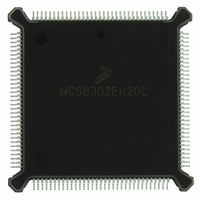
MC68302EH20C Freescale Semiconductor, MC68302EH20C Datasheet - Page 247

MC68302EH20C
Manufacturer Part Number
MC68302EH20C
Description
IC MPU MULTI-PROTOCOL 132-PQFP
Manufacturer
Freescale Semiconductor
Datasheets
1.MC68302AG20C.pdf
(4 pages)
2.MC68302AG20C.pdf
(2 pages)
3.MC68302AG20C.pdf
(13 pages)
4.MC68302EH20C.pdf
(481 pages)
Specifications of MC68302EH20C
Processor Type
M683xx 32-Bit
Speed
20MHz
Voltage
5V
Mounting Type
Surface Mount
Package / Case
132-MQFP, 132-PQFP
Family Name
M68000
Device Core
ColdFire
Device Core Size
32b
Frequency (max)
20MHz
Instruction Set Architecture
RISC
Supply Voltage 1 (typ)
5V
Operating Temp Range
0C to 70C
Operating Temperature Classification
Commercial
Mounting
Surface Mount
Pin Count
132
Package Type
PQFP
Lead Free Status / RoHS Status
Lead free / RoHS Compliant
Features
-
Lead Free Status / Rohs Status
Compliant
Available stocks
Company
Part Number
Manufacturer
Quantity
Price
Company:
Part Number:
MC68302EH20C
Manufacturer:
Freescale Semiconductor
Quantity:
10 000
Part Number:
MC68302EH20C
Manufacturer:
FREESCALE
Quantity:
20 000
Company:
Part Number:
MC68302EH20CB1
Manufacturer:
Freescale Semiconductor
Quantity:
10 000
Company:
Part Number:
MC68302EH20CR2
Manufacturer:
Freescale Semiconductor
Quantity:
10 000
- MC68302AG20C PDF datasheet
- MC68302AG20C PDF datasheet #2
- MC68302AG20C PDF datasheet #3
- MC68302EH20C PDF datasheet #4
- Current page: 247 of 481
- Download datasheet (2Mb)
transparent synchronization. Transparent synchronization gives the user bit-level control
over when the transmission and reception can begin.
The method of synchronization is controlled by the DIAG1–DIAG0 bits in the SCM, the EX-
SYN bit in the SCM, and, in some cases, the data synchronization register (DSR). The re-
sulting timing is dependent on the physical interface chosen.
Five ways exist to achieve transparent synchronization.
MOTOROLA
1. With the physical interface in the NMSI mode, the SCC may be configured with the EX-
2. With the physical interface in NMSI mode, the SCC may be configured with the EX-
3. If case 2 is used but the DIAG1–DIAG0 bits are set to normal operation, then the nor-
4. With the physical interface configured for PCM highway mode, the SCC may be con-
SYN bit set, and the DIAG1–DIAG0 bits set to software operation. In this case, the
CTS pin is ignored, and the CD pin is used to control both transmission and reception.
For the transmitter, once RTS is asserted and the transmitter samples CD as low, the
transmission will begin after a fixed 6.5 transmit clock delay. For the receiver, the first
valid bit of data received occurs one bit prior to the receive clock that sampled CD as
low. Note that CD is sampled on a rising TCLK for the transmitter and a rising RCLK
for the receiver.
Once CD is sampled as low by the receiver and transmitter, further toggling of CD will
have no effect since synchronization has already been achieved.
SYN bit cleared and the DIAG1–DIAG0 bits set to software operation. For the trans-
mitter, the transmission will begin without any synchronization. For the receiver,
reception will begin as soon as the receive data pattern matches the SYN1–SYN2 pat-
tern programmed into the DSR. Thus, the receiver uses an in-line synchronization
method.
mal operation characteristics as described in the SCM register also apply. The trans-
mitter will be controlled by the CTS pin, and the receiver will wait for the SYN1–SYN2
pattern once the CD pin is detected as low.
figured with the EXSYN bit set and the DIAG1–DIAG0 bits set to either software oper-
ation or normal operation. In this case, the L1SY1–L1SY0 pins carry out the
synchronization. For the transmitter, once data is preloaded into the transmit FIFO, the
rising edge of the L1SY1–L1SY0 pins will cause a transmission to occur. This trans-
mission will be comprised of one leading $FF byte, followed by the first bit of the trans-
mit buffer. For the receiver, reception will begin at the beginning of a time slot.
See D.8 Using the MC68302 Transparent Mode for timing dia-
grams and additional details concerning mode.
In cases 2 and 3 above, the SYN2 character is written into the
receive data buffer.
MC68302 USER’S MANUAL
NOTE
NOTE
Communications Processor (CP)
4-127
Related parts for MC68302EH20C
Image
Part Number
Description
Manufacturer
Datasheet
Request
R
Part Number:
Description:
Manufacturer:
Freescale Semiconductor, Inc
Datasheet:

Part Number:
Description:
MC68302 Configuring the Chip Selects on the MC68302
Manufacturer:
Motorola / Freescale Semiconductor

Part Number:
Description:
MC68302 Design Concept - Expanding Interrupts on the MC68302
Manufacturer:
Motorola / Freescale Semiconductor

Part Number:
Description:
MC68302 MC68302 Adapting a WAN Controller to a LAN Environment
Manufacturer:
Motorola / Freescale Semiconductor

Part Number:
Description:
MC68302 EKB Applications - Power Measurements on the MC68302
Manufacturer:
Motorola / Freescale Semiconductor

Part Number:
Description:
MC68302 Interfacing the MC68020 to a Slave MC68302
Manufacturer:
Motorola / Freescale Semiconductor

Part Number:
Description:
MC68302 MC68302 Software Performance
Manufacturer:
Motorola / Freescale Semiconductor

Part Number:
Description:
MC68302 Evaluating EDX on the ADS302
Manufacturer:
Motorola / Freescale Semiconductor

Part Number:
Description:
MC68302 Design Advisory #1 - MC68SC302 Passive ISDN Protocol Engine
Manufacturer:
Motorola / Freescale Semiconductor

Part Number:
Description:
MC68302, MC68360, and MPC860 Characteristics and Design Notes for Crystal Feedback Oscillators
Manufacturer:
Motorola / Freescale Semiconductor
Part Number:
Description:
Mc68302 Integrated Multi-protocol Processor
Manufacturer:
Freescale Semiconductor, Inc
Datasheet:
Part Number:
Description:
Manufacturer:
Freescale Semiconductor, Inc
Datasheet:
Part Number:
Description:
Manufacturer:
Freescale Semiconductor, Inc
Datasheet:
Part Number:
Description:
Manufacturer:
Freescale Semiconductor, Inc
Datasheet:
Part Number:
Description:
Manufacturer:
Freescale Semiconductor, Inc
Datasheet:


