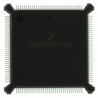
MC68302EH20C Freescale Semiconductor, MC68302EH20C Datasheet - Page 84

MC68302EH20C
Manufacturer Part Number
MC68302EH20C
Description
IC MPU MULTI-PROTOCOL 132-PQFP
Manufacturer
Freescale Semiconductor
Datasheets
1.MC68302AG20C.pdf
(4 pages)
2.MC68302AG20C.pdf
(2 pages)
3.MC68302AG20C.pdf
(13 pages)
4.MC68302EH20C.pdf
(481 pages)
Specifications of MC68302EH20C
Processor Type
M683xx 32-Bit
Speed
20MHz
Voltage
5V
Mounting Type
Surface Mount
Package / Case
132-MQFP, 132-PQFP
Family Name
M68000
Device Core
ColdFire
Device Core Size
32b
Frequency (max)
20MHz
Instruction Set Architecture
RISC
Supply Voltage 1 (typ)
5V
Operating Temp Range
0C to 70C
Operating Temperature Classification
Commercial
Mounting
Surface Mount
Pin Count
132
Package Type
PQFP
Lead Free Status / RoHS Status
Lead free / RoHS Compliant
Features
-
Lead Free Status / Rohs Status
Compliant
Available stocks
Company
Part Number
Manufacturer
Quantity
Price
Company:
Part Number:
MC68302EH20C
Manufacturer:
Freescale Semiconductor
Quantity:
10 000
Part Number:
MC68302EH20C
Manufacturer:
FREESCALE
Quantity:
20 000
Company:
Part Number:
MC68302EH20CB1
Manufacturer:
Freescale Semiconductor
Quantity:
10 000
Company:
Part Number:
MC68302EH20CR2
Manufacturer:
Freescale Semiconductor
Quantity:
10 000
- MC68302AG20C PDF datasheet
- MC68302AG20C PDF datasheet #2
- MC68302AG20C PDF datasheet #3
- MC68302EH20C PDF datasheet #4
- Current page: 84 of 481
- Download datasheet (2Mb)
System Integration Block (SIB)
nously with no wait states. The external master requests the M68000 bus using the BR pin
and is granted bus ownership. The external master must then access the RAM synchro-
nously with respect to the IMP system clock with zero or one wait state, or asynchronously
as determined by the EMWS and SAM bits in the system control register. Except for several
locations initialized by the CP, the dual-port RAM is undefined at power-on reset but is not
modified by successive resets. The RAM is divided into two parts: parameter RAM and sys-
tem RAM.
The 576-byte parameter RAM area includes pointers, counters, and registers used with the
serial ports. This area is accessed by the CP during communications processing. Any indi-
vidual locations not required in a given application may be used as general-purpose RAM.
The 576-byte system RAM is a general-purpose RAM, which may be used as M68000 data
and/or program RAM or CP microcode RAM. As data RAM, it can include serial port data
buffers or can be used for other purposes such as a no-wait-state cache for the M68000
core. As CP microcode RAM, it is used exclusively to store microcode for the CP main con-
troller, allowing the development of special protocols or protocol enhancements, under spe-
cial arrangement with Motorola. Appendix C discusses available offerings.
The RAM block diagram is shown in Figure 3-7. The M68000 core, the IDMA, and the ex-
ternal master access the RAM through the IMP bus interface unit (BIU) using the M68000
bus. When an access is made, the BIU generates a wait signal to the CP main controller to
prevent simultaneous access of the RAM. The CP main controller waits for one cycle to al-
low the RAM to service the M68000 bus cycle and then regenerates its RAM cycle. This
mechanism allows the RAM to be accessed synchronously by the M68000 core, IDMA, or
external master without wait states. Thus, during the four-clock M68000 memory cycle,
three internal accesses by the CP main controller may occur. The BIU also provides the
DTACK signal output when the RAM and on-chip registers are accessed by any M68000
bus master.
3-34
MC68302 USER’S MANUAL
MOTOROLA
Related parts for MC68302EH20C
Image
Part Number
Description
Manufacturer
Datasheet
Request
R
Part Number:
Description:
Manufacturer:
Freescale Semiconductor, Inc
Datasheet:

Part Number:
Description:
MC68302 Configuring the Chip Selects on the MC68302
Manufacturer:
Motorola / Freescale Semiconductor

Part Number:
Description:
MC68302 Design Concept - Expanding Interrupts on the MC68302
Manufacturer:
Motorola / Freescale Semiconductor

Part Number:
Description:
MC68302 MC68302 Adapting a WAN Controller to a LAN Environment
Manufacturer:
Motorola / Freescale Semiconductor

Part Number:
Description:
MC68302 EKB Applications - Power Measurements on the MC68302
Manufacturer:
Motorola / Freescale Semiconductor

Part Number:
Description:
MC68302 Interfacing the MC68020 to a Slave MC68302
Manufacturer:
Motorola / Freescale Semiconductor

Part Number:
Description:
MC68302 MC68302 Software Performance
Manufacturer:
Motorola / Freescale Semiconductor

Part Number:
Description:
MC68302 Evaluating EDX on the ADS302
Manufacturer:
Motorola / Freescale Semiconductor

Part Number:
Description:
MC68302 Design Advisory #1 - MC68SC302 Passive ISDN Protocol Engine
Manufacturer:
Motorola / Freescale Semiconductor

Part Number:
Description:
MC68302, MC68360, and MPC860 Characteristics and Design Notes for Crystal Feedback Oscillators
Manufacturer:
Motorola / Freescale Semiconductor
Part Number:
Description:
Mc68302 Integrated Multi-protocol Processor
Manufacturer:
Freescale Semiconductor, Inc
Datasheet:
Part Number:
Description:
Manufacturer:
Freescale Semiconductor, Inc
Datasheet:
Part Number:
Description:
Manufacturer:
Freescale Semiconductor, Inc
Datasheet:
Part Number:
Description:
Manufacturer:
Freescale Semiconductor, Inc
Datasheet:
Part Number:
Description:
Manufacturer:
Freescale Semiconductor, Inc
Datasheet:


