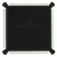
MC68302EH20C Freescale Semiconductor, MC68302EH20C Datasheet - Page 59

MC68302EH20C
Manufacturer Part Number
MC68302EH20C
Description
IC MPU MULTI-PROTOCOL 132-PQFP
Manufacturer
Freescale Semiconductor
Datasheets
1.MC68302AG20C.pdf
(4 pages)
2.MC68302AG20C.pdf
(2 pages)
3.MC68302AG20C.pdf
(13 pages)
4.MC68302EH20C.pdf
(481 pages)
Specifications of MC68302EH20C
Processor Type
M683xx 32-Bit
Speed
20MHz
Voltage
5V
Mounting Type
Surface Mount
Package / Case
132-MQFP, 132-PQFP
Family Name
M68000
Device Core
ColdFire
Device Core Size
32b
Frequency (max)
20MHz
Instruction Set Architecture
RISC
Supply Voltage 1 (typ)
5V
Operating Temp Range
0C to 70C
Operating Temperature Classification
Commercial
Mounting
Surface Mount
Pin Count
132
Package Type
PQFP
Lead Free Status / RoHS Status
Lead free / RoHS Compliant
Features
-
Lead Free Status / Rohs Status
Compliant
Available stocks
Company
Part Number
Manufacturer
Quantity
Price
Company:
Part Number:
MC68302EH20C
Manufacturer:
Freescale Semiconductor
Quantity:
10 000
Part Number:
MC68302EH20C
Manufacturer:
FREESCALE
Quantity:
20 000
Company:
Part Number:
MC68302EH20CB1
Manufacturer:
Freescale Semiconductor
Quantity:
10 000
Company:
Part Number:
MC68302EH20CR2
Manufacturer:
Freescale Semiconductor
Quantity:
10 000
- MC68302AG20C PDF datasheet
- MC68302AG20C PDF datasheet #2
- MC68302AG20C PDF datasheet #3
- MC68302EH20C PDF datasheet #4
- Current page: 59 of 481
- Download datasheet (2Mb)
3.1.4 IDMA Operational Description
Every IDMA operation involves the following steps: IDMA channel initialization, data trans-
fer, and block termination. In the initialization phase, the M68000 core (or external proces-
sor) loads the registers with control information, address pointers and transfer count, and
then starts the channel. In the transfer phase, the IDMA accepts requests for operand trans-
fers and provides addressing and bus control for the transfers. The termination phase oc-
curs when the operation is complete and the IDMA interrupts the M68000 core, if interrupts
are enabled.
3.1.4.1 Channel Initialization
To start a block transfer operation, the M68000 core must initialize IDMA registers with in-
formation describing the data block, device type, request generation method, and other spe-
cial control options. See 3.1.2 IDMA Registers (Independent DMA Controller) and 3.1.5
IDMA Programming for further details.
3.1.4.2 Data Transfer
The IDMA supports dual address transfers only. Thus, each operand transfer consists of a
source operand read and a destination operand write. The source operand is read from the
address contained in the SAPR into the DHR. When the source and destination operand siz-
es differ, the operand read may take up to two bus cycles to complete. The operand is then
written to the address contained in the DAPR. Again, this transfer may be up to two bus cy-
cles long. In this manner, various combinations of peripheral, memory, and operand sizes
may be used.
Source Operand Read
Destination Operand Write
MOTOROLA
During this cycle, the SAPR drives the address bus, the FCR drives the source function
codes, and the CMR drives the size control. The data is read from memory or the periph-
eral and placed temporarily into the data holding register (DHR) when the bus cycle is ter-
minated with DTACK. When the complete operand has been read, the SAPR is
incremented by one or two, depending on the address and size information. See 3.1.2.2
Source Address Pointer Register (SAPR) for more details.
During this cycle, the data in DHR is written to the device or memory selected by the ad-
dress from the DAPR, using the destination function codes from the FCR and the size
from the CMR. The same options exist for operand size and alignment as for the source
operand read. When the complete operand is written, the DAPR is incremented by one or
two, and the BCR is decremented by the number of bytes transferred. See 3.1.2.3 Desti-
nation Address Pointer Register (DAPR) and 3.1.2.5 Byte Count Register (BCR) for more
details.
When the SAPR and DAPR are programmed not to increment
and the bus width is 16 bits, the SAPR and DAPR addresses
must be even.
MC68302 USER’S MANUAL
NOTE
System Integration Block (SIB)
3-9
Related parts for MC68302EH20C
Image
Part Number
Description
Manufacturer
Datasheet
Request
R
Part Number:
Description:
Manufacturer:
Freescale Semiconductor, Inc
Datasheet:

Part Number:
Description:
MC68302 Configuring the Chip Selects on the MC68302
Manufacturer:
Motorola / Freescale Semiconductor

Part Number:
Description:
MC68302 Design Concept - Expanding Interrupts on the MC68302
Manufacturer:
Motorola / Freescale Semiconductor

Part Number:
Description:
MC68302 MC68302 Adapting a WAN Controller to a LAN Environment
Manufacturer:
Motorola / Freescale Semiconductor

Part Number:
Description:
MC68302 EKB Applications - Power Measurements on the MC68302
Manufacturer:
Motorola / Freescale Semiconductor

Part Number:
Description:
MC68302 Interfacing the MC68020 to a Slave MC68302
Manufacturer:
Motorola / Freescale Semiconductor

Part Number:
Description:
MC68302 MC68302 Software Performance
Manufacturer:
Motorola / Freescale Semiconductor

Part Number:
Description:
MC68302 Evaluating EDX on the ADS302
Manufacturer:
Motorola / Freescale Semiconductor

Part Number:
Description:
MC68302 Design Advisory #1 - MC68SC302 Passive ISDN Protocol Engine
Manufacturer:
Motorola / Freescale Semiconductor

Part Number:
Description:
MC68302, MC68360, and MPC860 Characteristics and Design Notes for Crystal Feedback Oscillators
Manufacturer:
Motorola / Freescale Semiconductor
Part Number:
Description:
Mc68302 Integrated Multi-protocol Processor
Manufacturer:
Freescale Semiconductor, Inc
Datasheet:
Part Number:
Description:
Manufacturer:
Freescale Semiconductor, Inc
Datasheet:
Part Number:
Description:
Manufacturer:
Freescale Semiconductor, Inc
Datasheet:
Part Number:
Description:
Manufacturer:
Freescale Semiconductor, Inc
Datasheet:
Part Number:
Description:
Manufacturer:
Freescale Semiconductor, Inc
Datasheet:


