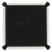
MC68302EH20C Freescale Semiconductor, MC68302EH20C Datasheet - Page 281

MC68302EH20C
Manufacturer Part Number
MC68302EH20C
Description
IC MPU MULTI-PROTOCOL 132-PQFP
Manufacturer
Freescale Semiconductor
Datasheets
1.MC68302AG20C.pdf
(4 pages)
2.MC68302AG20C.pdf
(2 pages)
3.MC68302AG20C.pdf
(13 pages)
4.MC68302EH20C.pdf
(481 pages)
Specifications of MC68302EH20C
Processor Type
M683xx 32-Bit
Speed
20MHz
Voltage
5V
Mounting Type
Surface Mount
Package / Case
132-MQFP, 132-PQFP
Family Name
M68000
Device Core
ColdFire
Device Core Size
32b
Frequency (max)
20MHz
Instruction Set Architecture
RISC
Supply Voltage 1 (typ)
5V
Operating Temp Range
0C to 70C
Operating Temperature Classification
Commercial
Mounting
Surface Mount
Pin Count
132
Package Type
PQFP
Lead Free Status / RoHS Status
Lead free / RoHS Compliant
Features
-
Lead Free Status / Rohs Status
Compliant
Available stocks
Company
Part Number
Manufacturer
Quantity
Price
Company:
Part Number:
MC68302EH20C
Manufacturer:
Freescale Semiconductor
Quantity:
10 000
Part Number:
MC68302EH20C
Manufacturer:
FREESCALE
Quantity:
20 000
Company:
Part Number:
MC68302EH20CB1
Manufacturer:
Freescale Semiconductor
Quantity:
10 000
Company:
Part Number:
MC68302EH20CR2
Manufacturer:
Freescale Semiconductor
Quantity:
10 000
- MC68302AG20C PDF datasheet
- MC68302AG20C PDF datasheet #2
- MC68302AG20C PDF datasheet #3
- MC68302EH20C PDF datasheet #4
- Current page: 281 of 481
- Download datasheet (2Mb)
RTS1/L1RQ/GCIDCL—Request to Send/Layer-1 Request/GCI Clock Out
BRG1—Baud Rate Generator 1
5.14 NMSI2 PORT OR PORT A PINS
The NMSI2 port or port A pins are shown in Figure 5-11.
These eight pins can be used either as the NMSI2 port or as a general-purpose parallel I/O
port. Each one of these pins can be configured individually to be general-purpose I/O pins
or a dedicated function in NMSI2. When they are used as NMSI2 pins, they function exactly
as the NMSI1 pins in NMSI mode.
The PA7 signal in dedicated mode becomes serial data strobe 2 (SDS2) in IDL and GCI
modes. In IDL/GCI modes, the SDS2–SDS1 outputs may be used to route the B1 and/or B2
channels to devices that do not support the IDL or GCI buses. This is configured in the SI-
MODE and SIMASK registers. If SCC2 is in NMSI mode, this pin operates as BRG2, the out-
put of the SCC2 baud rate generator, unless SDS2 is enabled to be asserted during the B1
or B2 channels of ISDN (bits SDC2–SDC1 of SIMODE). SDS2/BRG2 may be temporarily
disabled by configuring it as a general-purpose output pin. The input buffers have Schmitt
MOTOROLA
If SCC1 is programmed not to support CTS1 (in the SCC1 mode register), then this pin
may be used as an external interrupt source. The current value of the CTS1 pin may be
read in the SCCS1 register. See 4.5.8.3 SCC Status Register (SCCs) for details.
This output is the NMSI1 RTS signal in NMSI mode, the IDL request signal in IDL mode,
or the GCI data clock output in GCI mode.
RTS1 is asserted when SCC1 (in NMSI mode) has data or pad (flags or syncs) to transmit.
In GCI mode this pin is used to output the GCI data clock.
This output is always the baud rate generator clock of SCC1. (This pin used to be NC2.)
The BRG clock output on the BRG pins is 180 degrees out of phase with the internal BRG
clock output on the RCLK and TCLK pins. This statement applies to all BRG pins: BRG1,
BRG2, and BRG3. The BRG1 output can be disabled by setting bit 11 in the CKCR reg-
ister (see 3.9 Clock Control Register). When BRG1 is disabled the pin is driven high.
Figure 5-11. NMSI2 Port or Port A Pins
MC68302
MC68302 USER’S MANUAL
RXD2 / PA0
TXD2 / PA1
TCLK2 / PA3
CTS2 / PA4
CD2 / PA6
BRG2 / SDS2 / PA7
RCLK2 / PA2
RTS2 / PA5
Signal Description
5-17
Related parts for MC68302EH20C
Image
Part Number
Description
Manufacturer
Datasheet
Request
R
Part Number:
Description:
Manufacturer:
Freescale Semiconductor, Inc
Datasheet:

Part Number:
Description:
MC68302 Configuring the Chip Selects on the MC68302
Manufacturer:
Motorola / Freescale Semiconductor

Part Number:
Description:
MC68302 Design Concept - Expanding Interrupts on the MC68302
Manufacturer:
Motorola / Freescale Semiconductor

Part Number:
Description:
MC68302 MC68302 Adapting a WAN Controller to a LAN Environment
Manufacturer:
Motorola / Freescale Semiconductor

Part Number:
Description:
MC68302 EKB Applications - Power Measurements on the MC68302
Manufacturer:
Motorola / Freescale Semiconductor

Part Number:
Description:
MC68302 Interfacing the MC68020 to a Slave MC68302
Manufacturer:
Motorola / Freescale Semiconductor

Part Number:
Description:
MC68302 MC68302 Software Performance
Manufacturer:
Motorola / Freescale Semiconductor

Part Number:
Description:
MC68302 Evaluating EDX on the ADS302
Manufacturer:
Motorola / Freescale Semiconductor

Part Number:
Description:
MC68302 Design Advisory #1 - MC68SC302 Passive ISDN Protocol Engine
Manufacturer:
Motorola / Freescale Semiconductor

Part Number:
Description:
MC68302, MC68360, and MPC860 Characteristics and Design Notes for Crystal Feedback Oscillators
Manufacturer:
Motorola / Freescale Semiconductor
Part Number:
Description:
Mc68302 Integrated Multi-protocol Processor
Manufacturer:
Freescale Semiconductor, Inc
Datasheet:
Part Number:
Description:
Manufacturer:
Freescale Semiconductor, Inc
Datasheet:
Part Number:
Description:
Manufacturer:
Freescale Semiconductor, Inc
Datasheet:
Part Number:
Description:
Manufacturer:
Freescale Semiconductor, Inc
Datasheet:
Part Number:
Description:
Manufacturer:
Freescale Semiconductor, Inc
Datasheet:


