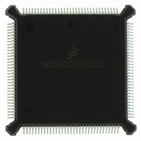
MC68302EH20C Freescale Semiconductor, MC68302EH20C Datasheet - Page 354

MC68302EH20C
Manufacturer Part Number
MC68302EH20C
Description
IC MPU MULTI-PROTOCOL 132-PQFP
Manufacturer
Freescale Semiconductor
Datasheets
1.MC68302AG20C.pdf
(4 pages)
2.MC68302AG20C.pdf
(2 pages)
3.MC68302AG20C.pdf
(13 pages)
4.MC68302EH20C.pdf
(481 pages)
Specifications of MC68302EH20C
Processor Type
M683xx 32-Bit
Speed
20MHz
Voltage
5V
Mounting Type
Surface Mount
Package / Case
132-MQFP, 132-PQFP
Family Name
M68000
Device Core
ColdFire
Device Core Size
32b
Frequency (max)
20MHz
Instruction Set Architecture
RISC
Supply Voltage 1 (typ)
5V
Operating Temp Range
0C to 70C
Operating Temperature Classification
Commercial
Mounting
Surface Mount
Pin Count
132
Package Type
PQFP
Lead Free Status / RoHS Status
Lead free / RoHS Compliant
Features
-
Lead Free Status / Rohs Status
Compliant
Available stocks
Company
Part Number
Manufacturer
Quantity
Price
Company:
Part Number:
MC68302EH20C
Manufacturer:
Freescale Semiconductor
Quantity:
10 000
Part Number:
MC68302EH20C
Manufacturer:
FREESCALE
Quantity:
20 000
Company:
Part Number:
MC68302EH20CB1
Manufacturer:
Freescale Semiconductor
Quantity:
10 000
Company:
Part Number:
MC68302EH20CR2
Manufacturer:
Freescale Semiconductor
Quantity:
10 000
- MC68302AG20C PDF datasheet
- MC68302AG20C PDF datasheet #2
- MC68302AG20C PDF datasheet #3
- MC68302EH20C PDF datasheet #4
- Current page: 354 of 481
- Download datasheet (2Mb)
MC68302 Applications
circuit will also place the MC68302 into reset if V
drops below a threshold, an advantage
cc
over a simple RC circuit.
D.1.3 Memory Interface
AS, R/W, UDS, LDS, A23–A1, D15–D0, CS0, and CS1 are used in the memory interface.
The bidirectional control signals have pullups so that they are inactive when the MC68302
is not actively driving them. CS0 and CS1 are only outputs and do not need pullups.
DTACK is generated internally by the wait-state generation logic, and therefore it does not
need to be externally connected. It is driven by the wait-state generation logic during chip-
select accesses and is pulled up externally through a resistor.
BCLR is an open-drain signal that is output by the MC68302 when the SDMA requests the
bus or (if enabled) when an interrupt request is pending. It is therefore pulled up externally.
D.1.4 Memory Circuit
The EPROM design is a straight connection. Larger EPROM sizes may be easily substitut-
ed; it is also possible to use a single 16-bit EPROM, if desired, and reduce the component
count by one.
CS0 is used to select the EPROM since CS0 is designed to be used for a boot ROM. CS0
comes up enabled for the first 8 kbytes of the system address space. Before the program
jumps outside of this space, it should configure the CS0 range for 32 kbytes and enable the
RAM chip select to cover the RAM range and desired starting address. To switch the RAM
down to low-order memory to allow exception vectors to be altered, see D.2 Switching the
External ROM and RAM Using the MC68302 .
LDS and UDS define the lower and upper bytes of the program word, respectively, and are
connected to the EPROM output enable.
The RAM design is similar to the EPROM design, except that the R/W signal is used to qual-
ify the output enable and the LDS/UDS signals are used to qualify whether to write the par-
ticular byte of the data word (the M68000 supports byte operations).
CS1 is used to select the RAM.
No external buffers are required in this small system design.
D.1.5 Memory Timing Analysis
The design as shown will work with zero wait states with a 100-ns EPROM and a static RAM,
such as the MCM6202. The RAM writes are controlled by the enable (E) rather than by the
write (W). Two of the MC68302 required specifications deserve special note.
The time between CS low and data valid must be calculated for proper timing of read cycles.
This time is approximately 2 1/2 clocks. CS is asserted by the MC68302 after the rising edge
of S2. Data must be valid a setup time before the S6 falling edge. Thus, for a 16.67-MHz
device, the equation for the time between CS low and data valid is as follows:
D-4
MC68302 USER’S MANUAL
MOTOROLA
Related parts for MC68302EH20C
Image
Part Number
Description
Manufacturer
Datasheet
Request
R
Part Number:
Description:
Manufacturer:
Freescale Semiconductor, Inc
Datasheet:

Part Number:
Description:
MC68302 Configuring the Chip Selects on the MC68302
Manufacturer:
Motorola / Freescale Semiconductor

Part Number:
Description:
MC68302 Design Concept - Expanding Interrupts on the MC68302
Manufacturer:
Motorola / Freescale Semiconductor

Part Number:
Description:
MC68302 MC68302 Adapting a WAN Controller to a LAN Environment
Manufacturer:
Motorola / Freescale Semiconductor

Part Number:
Description:
MC68302 EKB Applications - Power Measurements on the MC68302
Manufacturer:
Motorola / Freescale Semiconductor

Part Number:
Description:
MC68302 Interfacing the MC68020 to a Slave MC68302
Manufacturer:
Motorola / Freescale Semiconductor

Part Number:
Description:
MC68302 MC68302 Software Performance
Manufacturer:
Motorola / Freescale Semiconductor

Part Number:
Description:
MC68302 Evaluating EDX on the ADS302
Manufacturer:
Motorola / Freescale Semiconductor

Part Number:
Description:
MC68302 Design Advisory #1 - MC68SC302 Passive ISDN Protocol Engine
Manufacturer:
Motorola / Freescale Semiconductor

Part Number:
Description:
MC68302, MC68360, and MPC860 Characteristics and Design Notes for Crystal Feedback Oscillators
Manufacturer:
Motorola / Freescale Semiconductor
Part Number:
Description:
Mc68302 Integrated Multi-protocol Processor
Manufacturer:
Freescale Semiconductor, Inc
Datasheet:
Part Number:
Description:
Manufacturer:
Freescale Semiconductor, Inc
Datasheet:
Part Number:
Description:
Manufacturer:
Freescale Semiconductor, Inc
Datasheet:
Part Number:
Description:
Manufacturer:
Freescale Semiconductor, Inc
Datasheet:
Part Number:
Description:
Manufacturer:
Freescale Semiconductor, Inc
Datasheet:


