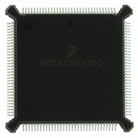
MC68302EH20C Freescale Semiconductor, MC68302EH20C Datasheet - Page 81

MC68302EH20C
Manufacturer Part Number
MC68302EH20C
Description
IC MPU MULTI-PROTOCOL 132-PQFP
Manufacturer
Freescale Semiconductor
Datasheets
1.MC68302AG20C.pdf
(4 pages)
2.MC68302AG20C.pdf
(2 pages)
3.MC68302AG20C.pdf
(13 pages)
4.MC68302EH20C.pdf
(481 pages)
Specifications of MC68302EH20C
Processor Type
M683xx 32-Bit
Speed
20MHz
Voltage
5V
Mounting Type
Surface Mount
Package / Case
132-MQFP, 132-PQFP
Family Name
M68000
Device Core
ColdFire
Device Core Size
32b
Frequency (max)
20MHz
Instruction Set Architecture
RISC
Supply Voltage 1 (typ)
5V
Operating Temp Range
0C to 70C
Operating Temperature Classification
Commercial
Mounting
Surface Mount
Pin Count
132
Package Type
PQFP
Lead Free Status / RoHS Status
Lead free / RoHS Compliant
Features
-
Lead Free Status / Rohs Status
Compliant
Available stocks
Company
Part Number
Manufacturer
Quantity
Price
Company:
Part Number:
MC68302EH20C
Manufacturer:
Freescale Semiconductor
Quantity:
10 000
Part Number:
MC68302EH20C
Manufacturer:
FREESCALE
Quantity:
20 000
Company:
Part Number:
MC68302EH20CB1
Manufacturer:
Freescale Semiconductor
Quantity:
10 000
Company:
Part Number:
MC68302EH20CR2
Manufacturer:
Freescale Semiconductor
Quantity:
10 000
- MC68302AG20C PDF datasheet
- MC68302AG20C PDF datasheet #2
- MC68302AG20C PDF datasheet #3
- MC68302EH20C PDF datasheet #4
- Current page: 81 of 481
- Download datasheet (2Mb)
now receives as its input, given that some of its pins have been reassigned, is shown in Ta-
ble 3-6. If an input pin to a channel (for example CD2 or CTS2) is used as a general-purpose
I/O pin, then the input to the peripheral is automatically connected internally to V
based on the pin's function. This does not affect the operation of the port pins in their gen-
eral-purpose I/O function.
3.3.2 Port B
Port B has 12 pins. PB7–PB0 may be configured as general-purpose I/O pins or as dedicat-
ed peripheral interface pins; whereas, PB11–PB8 are always maintained as four general-
purpose pins, each with interrupt capability.
3.3.2.1 PB7–PB0
Each port B pin may be configured as a general-purpose I/O pin or as a dedicated peripheral
interface pin. PB7–PB0 functions exactly like PA15–PA0, except that PB7–PB0 is controlled
by the port B control register (PBCNT), the port B data direction register (PBDDR), and the
port B data register (PBDAT), and PB7 is configured as an open-drain output (WDOG) upon
total system reset.
MOTOROLA
If the DREQ/PA13 pin is selected to be PA13, then DREQ is tied
low. If the IDMA is programmed for external requests, then it al-
ways recognizes an external request, and the entire block will be
transferred in one burst.
# Allows a single external clock source on the RCLK pin to clock both
PACNT Bit = 1
Pin Function
the SCC receiver and transmitter.
SDS2/BRG2
RCLK2
RCLK3
TCLK2
TCLK3
DREQ
DONE
RXD2
RXD3
BRG3
DACK
TXD2
CTS2
RTS2
TXD3
CD2
Table 3-6. Port A Pin Functions
MC68302 USER’S MANUAL
PACNT Bit = 0
Pin Function
PA10
PA11
PA12
PA13
PA14
PA15
PAO
PA1
PA2
PA3
PA4
PA5
PA6
PA7
PA8
PA9
NOTE
SCC2/SCC3/IDMA
Input to
RCLK2 #
RCLK3 #
GND
GND
GND
GND
GND
GND
GND
V DD
—
—
—
—
—
—
System Integration Block (SIB)
DD
or GND,
3-31
Related parts for MC68302EH20C
Image
Part Number
Description
Manufacturer
Datasheet
Request
R
Part Number:
Description:
Manufacturer:
Freescale Semiconductor, Inc
Datasheet:

Part Number:
Description:
MC68302 Configuring the Chip Selects on the MC68302
Manufacturer:
Motorola / Freescale Semiconductor

Part Number:
Description:
MC68302 Design Concept - Expanding Interrupts on the MC68302
Manufacturer:
Motorola / Freescale Semiconductor

Part Number:
Description:
MC68302 MC68302 Adapting a WAN Controller to a LAN Environment
Manufacturer:
Motorola / Freescale Semiconductor

Part Number:
Description:
MC68302 EKB Applications - Power Measurements on the MC68302
Manufacturer:
Motorola / Freescale Semiconductor

Part Number:
Description:
MC68302 Interfacing the MC68020 to a Slave MC68302
Manufacturer:
Motorola / Freescale Semiconductor

Part Number:
Description:
MC68302 MC68302 Software Performance
Manufacturer:
Motorola / Freescale Semiconductor

Part Number:
Description:
MC68302 Evaluating EDX on the ADS302
Manufacturer:
Motorola / Freescale Semiconductor

Part Number:
Description:
MC68302 Design Advisory #1 - MC68SC302 Passive ISDN Protocol Engine
Manufacturer:
Motorola / Freescale Semiconductor

Part Number:
Description:
MC68302, MC68360, and MPC860 Characteristics and Design Notes for Crystal Feedback Oscillators
Manufacturer:
Motorola / Freescale Semiconductor
Part Number:
Description:
Mc68302 Integrated Multi-protocol Processor
Manufacturer:
Freescale Semiconductor, Inc
Datasheet:
Part Number:
Description:
Manufacturer:
Freescale Semiconductor, Inc
Datasheet:
Part Number:
Description:
Manufacturer:
Freescale Semiconductor, Inc
Datasheet:
Part Number:
Description:
Manufacturer:
Freescale Semiconductor, Inc
Datasheet:
Part Number:
Description:
Manufacturer:
Freescale Semiconductor, Inc
Datasheet:


