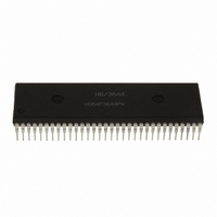
HD6473258P10 Renesas Electronics America, HD6473258P10 Datasheet - Page 67

HD6473258P10
Manufacturer Part Number
HD6473258P10
Description
IC H8 MCU OTP 32K 64DIP
Manufacturer
Renesas Electronics America
Series
H8® H8/325r
Datasheet
1.HD6413238F10.pdf
(301 pages)
Specifications of HD6473258P10
Core Processor
H8/300
Core Size
8-Bit
Speed
10MHz
Connectivity
SCI, UART/USART
Number Of I /o
53
Program Memory Size
32KB (32K x 8)
Program Memory Type
OTP
Ram Size
1K x 8
Voltage - Supply (vcc/vdd)
4.5 V ~ 5.5 V
Oscillator Type
External
Operating Temperature
-20°C ~ 75°C
Package / Case
64-DIP
Lead Free Status / RoHS Status
Contains lead / RoHS non-compliant
Eeprom Size
-
Data Converters
-
Peripherals
-
Available stocks
Company
Part Number
Manufacturer
Quantity
Price
Company:
Part Number:
HD6473258P10
Manufacturer:
EXEL
Quantity:
6 218
Company:
Part Number:
HD6473258P10V
Manufacturer:
RENESAS
Quantity:
600
Part Number:
HD6473258P10V
Manufacturer:
HITACHI/日立
Quantity:
20 000
- Current page: 67 of 301
- Download datasheet (2Mb)
3.7.2 Access to On-Chip Register Field and External Devices
The on-chip register field (I/O ports, dual-port RAM, on-chip supporting module registers, etc.) and
external devices are accessed in a cycle consisting of three states: T
data can be accessed per cycle, via an 8-bit data bus. Access to word data or instruction codes
requires two consecutive cycles (six states).
Wait States: If requested, additional wait states (T
pin is sampled at the center of state T
is also sampled at the center of each wait state and if it is still Low, another wait state is inserted.
An external device can have any number of wait states inserted by holding WAIT Low for the
necessary duration.
The bus cycle for the MOVTPE and MOVFPE instructions will be described in section 15,
"E-Clock Interface."
Figure 3-15 shows the access cycle for the on-chip register field. Figure 3-16 shows the associated
pin states. Figures 3-17 (a) and (b) show the read and write access timing for external devices.
Internal address bus
Internal Read signal
Internal data bus (read)
Internal Write signal
Internal data bus (write)
Ø
Figure 3-15. On-Chip Register Field Access Cycle
2
. If it is Low, a wait state is inserted after T
T1 state
58
W
) are inserted between T
Bus cycle
T2 state
Address
Read data
Write data
1
, T
2
, and T
T3 state
2
and T
3
. Only one byte of
2
. The WAIT pin
3
. The WAIT
Related parts for HD6473258P10
Image
Part Number
Description
Manufacturer
Datasheet
Request
R

Part Number:
Description:
KIT STARTER FOR M16C/29
Manufacturer:
Renesas Electronics America
Datasheet:

Part Number:
Description:
KIT STARTER FOR R8C/2D
Manufacturer:
Renesas Electronics America
Datasheet:

Part Number:
Description:
R0K33062P STARTER KIT
Manufacturer:
Renesas Electronics America
Datasheet:

Part Number:
Description:
KIT STARTER FOR R8C/23 E8A
Manufacturer:
Renesas Electronics America
Datasheet:

Part Number:
Description:
KIT STARTER FOR R8C/25
Manufacturer:
Renesas Electronics America
Datasheet:

Part Number:
Description:
KIT STARTER H8S2456 SHARPE DSPLY
Manufacturer:
Renesas Electronics America
Datasheet:

Part Number:
Description:
KIT STARTER FOR R8C38C
Manufacturer:
Renesas Electronics America
Datasheet:

Part Number:
Description:
KIT STARTER FOR R8C35C
Manufacturer:
Renesas Electronics America
Datasheet:

Part Number:
Description:
KIT STARTER FOR R8CL3AC+LCD APPS
Manufacturer:
Renesas Electronics America
Datasheet:

Part Number:
Description:
KIT STARTER FOR RX610
Manufacturer:
Renesas Electronics America
Datasheet:

Part Number:
Description:
KIT STARTER FOR R32C/118
Manufacturer:
Renesas Electronics America
Datasheet:

Part Number:
Description:
KIT DEV RSK-R8C/26-29
Manufacturer:
Renesas Electronics America
Datasheet:

Part Number:
Description:
KIT STARTER FOR SH7124
Manufacturer:
Renesas Electronics America
Datasheet:

Part Number:
Description:
KIT STARTER FOR H8SX/1622
Manufacturer:
Renesas Electronics America
Datasheet:

Part Number:
Description:
KIT DEV FOR SH7203
Manufacturer:
Renesas Electronics America
Datasheet:


