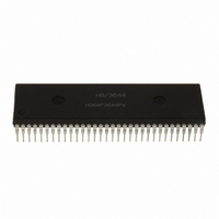
HD6473258P10 Renesas Electronics America, HD6473258P10 Datasheet - Page 231

HD6473258P10
Manufacturer Part Number
HD6473258P10
Description
IC H8 MCU OTP 32K 64DIP
Manufacturer
Renesas Electronics America
Series
H8® H8/325r
Datasheet
1.HD6413238F10.pdf
(301 pages)
Specifications of HD6473258P10
Core Processor
H8/300
Core Size
8-Bit
Speed
10MHz
Connectivity
SCI, UART/USART
Number Of I /o
53
Program Memory Size
32KB (32K x 8)
Program Memory Type
OTP
Ram Size
1K x 8
Voltage - Supply (vcc/vdd)
4.5 V ~ 5.5 V
Oscillator Type
External
Operating Temperature
-20°C ~ 75°C
Package / Case
64-DIP
Lead Free Status / RoHS Status
Contains lead / RoHS non-compliant
Eeprom Size
-
Data Converters
-
Peripherals
-
Available stocks
Company
Part Number
Manufacturer
Quantity
Price
Company:
Part Number:
HD6473258P10
Manufacturer:
EXEL
Quantity:
6 218
Company:
Part Number:
HD6473258P10V
Manufacturer:
RENESAS
Quantity:
600
Part Number:
HD6473258P10V
Manufacturer:
HITACHI/日立
Quantity:
20 000
- Current page: 231 of 301
- Download datasheet (2Mb)
Section 13. E-Clock Interface
13.1 Overview
For interfacing to peripheral devices that require it, the H8/325 series can generate an E clock
output. Special instructions (MOVTPE, MOVFPE) perform data transfers synchronized with the E
clock.
The E clock is created by dividing the system clock (Ø) by 8. The E clock is output at the P4
pin
7
when the P4
DDR bit in the port 4 data direction register (P4DDR) is set to 1. It is output only in
7
the expanded modes (mode 1 and mode 2); it is not output in the single-chip mode. Output begins
immediately after a reset.
When the CPU executes an instruction that synchronizes with the E clock, the address strobe (AS),
the address on the address bus, and the IOS signal are output as usual, but the RD and WR signal
lines and the data bus do not become active until the falling edge of the E clock is detected. The
length of the access cycle for an instruction synchronized with the E clock accordingly varies from
9 to 16 states. Figures 15-1 and 15-2 show the timing in the cases of maximum and minimum
synchronization delay.
It is not possible to insert wait states (T
) during the execution of an instruction synchronized with
w
the E clock by input at the WAIT pin.
227
Related parts for HD6473258P10
Image
Part Number
Description
Manufacturer
Datasheet
Request
R

Part Number:
Description:
KIT STARTER FOR M16C/29
Manufacturer:
Renesas Electronics America
Datasheet:

Part Number:
Description:
KIT STARTER FOR R8C/2D
Manufacturer:
Renesas Electronics America
Datasheet:

Part Number:
Description:
R0K33062P STARTER KIT
Manufacturer:
Renesas Electronics America
Datasheet:

Part Number:
Description:
KIT STARTER FOR R8C/23 E8A
Manufacturer:
Renesas Electronics America
Datasheet:

Part Number:
Description:
KIT STARTER FOR R8C/25
Manufacturer:
Renesas Electronics America
Datasheet:

Part Number:
Description:
KIT STARTER H8S2456 SHARPE DSPLY
Manufacturer:
Renesas Electronics America
Datasheet:

Part Number:
Description:
KIT STARTER FOR R8C38C
Manufacturer:
Renesas Electronics America
Datasheet:

Part Number:
Description:
KIT STARTER FOR R8C35C
Manufacturer:
Renesas Electronics America
Datasheet:

Part Number:
Description:
KIT STARTER FOR R8CL3AC+LCD APPS
Manufacturer:
Renesas Electronics America
Datasheet:

Part Number:
Description:
KIT STARTER FOR RX610
Manufacturer:
Renesas Electronics America
Datasheet:

Part Number:
Description:
KIT STARTER FOR R32C/118
Manufacturer:
Renesas Electronics America
Datasheet:

Part Number:
Description:
KIT DEV RSK-R8C/26-29
Manufacturer:
Renesas Electronics America
Datasheet:

Part Number:
Description:
KIT STARTER FOR SH7124
Manufacturer:
Renesas Electronics America
Datasheet:

Part Number:
Description:
KIT STARTER FOR H8SX/1622
Manufacturer:
Renesas Electronics America
Datasheet:

Part Number:
Description:
KIT DEV FOR SH7203
Manufacturer:
Renesas Electronics America
Datasheet:


