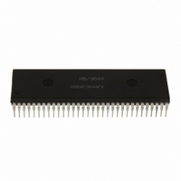
HD6473258P10 Renesas Electronics America, HD6473258P10 Datasheet - Page 105

HD6473258P10
Manufacturer Part Number
HD6473258P10
Description
IC H8 MCU OTP 32K 64DIP
Manufacturer
Renesas Electronics America
Series
H8® H8/325r
Datasheet
1.HD6413238F10.pdf
(301 pages)
Specifications of HD6473258P10
Core Processor
H8/300
Core Size
8-Bit
Speed
10MHz
Connectivity
SCI, UART/USART
Number Of I /o
53
Program Memory Size
32KB (32K x 8)
Program Memory Type
OTP
Ram Size
1K x 8
Voltage - Supply (vcc/vdd)
4.5 V ~ 5.5 V
Oscillator Type
External
Operating Temperature
-20°C ~ 75°C
Package / Case
64-DIP
Lead Free Status / RoHS Status
Contains lead / RoHS non-compliant
Eeprom Size
-
Data Converters
-
Peripherals
-
Available stocks
Company
Part Number
Manufacturer
Quantity
Price
Company:
Part Number:
HD6473258P10
Manufacturer:
EXEL
Quantity:
6 218
Company:
Part Number:
HD6473258P10V
Manufacturer:
RENESAS
Quantity:
600
Part Number:
HD6473258P10V
Manufacturer:
HITACHI/日立
Quantity:
20 000
- Current page: 105 of 301
- Download datasheet (2Mb)
Pins P5
serial transmit data (TxD). When used for TxD output, these pins are unaffected by the values in
P5DDR and P5DR, and their MOS pull-ups are automatically turned off.
Pins P5
receive data (RxD). When used for RxD input, these pins are unaffected by P5DDR and P5DR,
except that software can turn on their MOS pull-ups by clearing their data direction bits to 0 and
setting their data bits to 1.
Pins P5
input or output (SCK). When used for SCK output, these pins are unaffected by P5DDR and P5DR.
When these pins are used for SCK input, software can turn on their MOS pull-ups by clearing their
data direction bits to 0 and setting their data bits to 1.
Reset and Hardware Standby Mode: P5DDR and P5DR are cleared to all 0 and the serial control
registers are initialized. All pins are placed in the input port (high-impedance) state with the MOS
pull-ups off.
Software Standby Mode: The serial control registers are initialized but P5DDR and P5DR remain
in their previous states. All pins become input or output port pins depending on the setting of
P5DDR. Output pins output the values in P5DR. The MOS pull-ups of input pins are on or off
depending on the values in P5DR.
Figures 5-8 to 5-10 show schematic diagrams of port 5.
0
1
2
and P5
and P5
and P5
3
4
5
: These pins can be used for general-purpose input or output, or for output of
: These pins can be used for general-purpose input or output, or for input of serial
: These pins can be used for general-purpose input or output, or for serial clock
96
Related parts for HD6473258P10
Image
Part Number
Description
Manufacturer
Datasheet
Request
R

Part Number:
Description:
KIT STARTER FOR M16C/29
Manufacturer:
Renesas Electronics America
Datasheet:

Part Number:
Description:
KIT STARTER FOR R8C/2D
Manufacturer:
Renesas Electronics America
Datasheet:

Part Number:
Description:
R0K33062P STARTER KIT
Manufacturer:
Renesas Electronics America
Datasheet:

Part Number:
Description:
KIT STARTER FOR R8C/23 E8A
Manufacturer:
Renesas Electronics America
Datasheet:

Part Number:
Description:
KIT STARTER FOR R8C/25
Manufacturer:
Renesas Electronics America
Datasheet:

Part Number:
Description:
KIT STARTER H8S2456 SHARPE DSPLY
Manufacturer:
Renesas Electronics America
Datasheet:

Part Number:
Description:
KIT STARTER FOR R8C38C
Manufacturer:
Renesas Electronics America
Datasheet:

Part Number:
Description:
KIT STARTER FOR R8C35C
Manufacturer:
Renesas Electronics America
Datasheet:

Part Number:
Description:
KIT STARTER FOR R8CL3AC+LCD APPS
Manufacturer:
Renesas Electronics America
Datasheet:

Part Number:
Description:
KIT STARTER FOR RX610
Manufacturer:
Renesas Electronics America
Datasheet:

Part Number:
Description:
KIT STARTER FOR R32C/118
Manufacturer:
Renesas Electronics America
Datasheet:

Part Number:
Description:
KIT DEV RSK-R8C/26-29
Manufacturer:
Renesas Electronics America
Datasheet:

Part Number:
Description:
KIT STARTER FOR SH7124
Manufacturer:
Renesas Electronics America
Datasheet:

Part Number:
Description:
KIT STARTER FOR H8SX/1622
Manufacturer:
Renesas Electronics America
Datasheet:

Part Number:
Description:
KIT DEV FOR SH7203
Manufacturer:
Renesas Electronics America
Datasheet:


