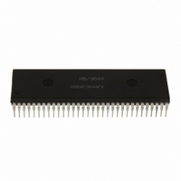
HD6473258P10 Renesas Electronics America, HD6473258P10 Datasheet - Page 193

HD6473258P10
Manufacturer Part Number
HD6473258P10
Description
IC H8 MCU OTP 32K 64DIP
Manufacturer
Renesas Electronics America
Series
H8® H8/325r
Datasheet
1.HD6413238F10.pdf
(301 pages)
Specifications of HD6473258P10
Core Processor
H8/300
Core Size
8-Bit
Speed
10MHz
Connectivity
SCI, UART/USART
Number Of I /o
53
Program Memory Size
32KB (32K x 8)
Program Memory Type
OTP
Ram Size
1K x 8
Voltage - Supply (vcc/vdd)
4.5 V ~ 5.5 V
Oscillator Type
External
Operating Temperature
-20°C ~ 75°C
Package / Case
64-DIP
Lead Free Status / RoHS Status
Contains lead / RoHS non-compliant
Eeprom Size
-
Data Converters
-
Peripherals
-
Available stocks
Company
Part Number
Manufacturer
Quantity
Price
Company:
Part Number:
HD6473258P10
Manufacturer:
EXEL
Quantity:
6 218
Company:
Part Number:
HD6473258P10V
Manufacturer:
RENESAS
Quantity:
600
Part Number:
HD6473258P10V
Manufacturer:
HITACHI/日立
Quantity:
20 000
- Current page: 193 of 301
- Download datasheet (2Mb)
(3) Data Transmission and Reception
• SCI Initialization: Before data can be transmitted or received, the SCI must be initialized by
The TE and RE bits must both be cleared to 0 whenever the operating mode or data format is
changed.
After changing the operating mode or data format, before setting the TE and RE bits to 1 software
must wait for at least the transfer time for 1 bit at the selected baud rate, to make sure the SCI is
initialized. If an external clock is used, the clock must not be stopped.
When clearing the TDRE bit during data transmission, to assure transfer of the correct data, do not
clear the TDRE bit until after writing data in the TDR. Similarly, in receiving data, do not clear the
RDRF bit until after reading data from the RDR.
• Data Transmission: The procedure for transmitting data is as follows.
software. To initialize the SCI, software must clear the TE and RE bits to 0, then execute the
following procedure.
Set the desired communication format in the SMR.
Write the value corresponding to the desired baud rate in the BRR. (This step is not necessary
if an external clock is used.)
Select the clock and enable desired interrupts in the SCR.
Set the TE and/or RE bit in the SCR to 1.
Set up the desired transmitting conditions in the SMR, SCR, and BRR.
Set the TE bit in the SCR to 1.
The TxD pin will automatically be switched to output and one frame* of all 1’s will be
transmitted, after which the SCI is ready to transmit data.
Check that the TDRE bit is set to 1, then write the first byte of transmit data in the TDR. Next
clear the TDRE bit to 0.
186
Related parts for HD6473258P10
Image
Part Number
Description
Manufacturer
Datasheet
Request
R

Part Number:
Description:
KIT STARTER FOR M16C/29
Manufacturer:
Renesas Electronics America
Datasheet:

Part Number:
Description:
KIT STARTER FOR R8C/2D
Manufacturer:
Renesas Electronics America
Datasheet:

Part Number:
Description:
R0K33062P STARTER KIT
Manufacturer:
Renesas Electronics America
Datasheet:

Part Number:
Description:
KIT STARTER FOR R8C/23 E8A
Manufacturer:
Renesas Electronics America
Datasheet:

Part Number:
Description:
KIT STARTER FOR R8C/25
Manufacturer:
Renesas Electronics America
Datasheet:

Part Number:
Description:
KIT STARTER H8S2456 SHARPE DSPLY
Manufacturer:
Renesas Electronics America
Datasheet:

Part Number:
Description:
KIT STARTER FOR R8C38C
Manufacturer:
Renesas Electronics America
Datasheet:

Part Number:
Description:
KIT STARTER FOR R8C35C
Manufacturer:
Renesas Electronics America
Datasheet:

Part Number:
Description:
KIT STARTER FOR R8CL3AC+LCD APPS
Manufacturer:
Renesas Electronics America
Datasheet:

Part Number:
Description:
KIT STARTER FOR RX610
Manufacturer:
Renesas Electronics America
Datasheet:

Part Number:
Description:
KIT STARTER FOR R32C/118
Manufacturer:
Renesas Electronics America
Datasheet:

Part Number:
Description:
KIT DEV RSK-R8C/26-29
Manufacturer:
Renesas Electronics America
Datasheet:

Part Number:
Description:
KIT STARTER FOR SH7124
Manufacturer:
Renesas Electronics America
Datasheet:

Part Number:
Description:
KIT STARTER FOR H8SX/1622
Manufacturer:
Renesas Electronics America
Datasheet:

Part Number:
Description:
KIT DEV FOR SH7203
Manufacturer:
Renesas Electronics America
Datasheet:


