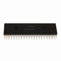
HD6473258P10 Renesas Electronics America, HD6473258P10 Datasheet - Page 197

HD6473258P10
Manufacturer Part Number
HD6473258P10
Description
IC H8 MCU OTP 32K 64DIP
Manufacturer
Renesas Electronics America
Series
H8® H8/325r
Datasheet
1.HD6413238F10.pdf
(301 pages)
Specifications of HD6473258P10
Core Processor
H8/300
Core Size
8-Bit
Speed
10MHz
Connectivity
SCI, UART/USART
Number Of I /o
53
Program Memory Size
32KB (32K x 8)
Program Memory Type
OTP
Ram Size
1K x 8
Voltage - Supply (vcc/vdd)
4.5 V ~ 5.5 V
Oscillator Type
External
Operating Temperature
-20°C ~ 75°C
Package / Case
64-DIP
Lead Free Status / RoHS Status
Contains lead / RoHS non-compliant
Eeprom Size
-
Data Converters
-
Peripherals
-
Available stocks
Company
Part Number
Manufacturer
Quantity
Price
Company:
Part Number:
HD6473258P10
Manufacturer:
EXEL
Quantity:
6 218
Company:
Part Number:
HD6473258P10V
Manufacturer:
RENESAS
Quantity:
600
Part Number:
HD6473258P10V
Manufacturer:
HITACHI/日立
Quantity:
20 000
- Current page: 197 of 301
- Download datasheet (2Mb)
When clearing the TDRE bit during data transmission, to assure correct data transfer, do not clear
the TDRE bit until after writing data in the TDR. Similarly, in receiving data, do not clear the
RDRF bit until after reading data from the RDR.
• Data Transmission: The procedure for transmitting data is as follows.
The TDR and TSR function as a double buffer. Continuous data transmission can be achieved by
writing the next transmit data in the TDR and clearing the TDRE bit to 0 while the SCI is
transmitting the current data from the TSR.
If an internal clock source is selected, after transferring the transmit data from the TDR to the TSR,
while transmitting the data from the TSR the SCI also outputs a serial clock signal at the SCK pin.
When all data bits in the TSR have been transmitted, if the TDR is empty (TDRE = 1), serial clock
output is suspended until the next data byte is written in the TDR and the TDRE bit is cleared to 0.
During this interval the TxD pin continues to output the value of the last bit of the previous data.
If the external clock source is selected, data transmission is synchronized with the clock signal
input at the SCK pin. When all data bits in the TSR have been transmitted, if the TDR is empty
(TDRE = 1) but external clock pulses continue to arrive, the TxD pin outputs the value of last bit of
the previous data.
• Data Reception: The procedure for receiving data is as follows.
Set up the desired transmitting conditions in the SMR, BRR, and SCR.
Set the TE bit in the SCR to 1.
The TxD pin will automatically be switched to output, after which the SCI is ready to transmit
data.
Check that the TDRE bit is set to 1, then write the first byte of transmit data in the TDR. Next
clear the TDRE bit to 0.
The first byte of transmit data is transferred from the TDR to the TSR and sent, each bit
synchronized with a clock pulse. Bit 0 is sent first.
Transfer of the transmit data from the TDR to the TSR makes the TDR empty, so the TDRE bit
is set to 1. If the TIE bit is set to 1, a transmit-end interrupt (TXI) is requested.
190
Related parts for HD6473258P10
Image
Part Number
Description
Manufacturer
Datasheet
Request
R

Part Number:
Description:
KIT STARTER FOR M16C/29
Manufacturer:
Renesas Electronics America
Datasheet:

Part Number:
Description:
KIT STARTER FOR R8C/2D
Manufacturer:
Renesas Electronics America
Datasheet:

Part Number:
Description:
R0K33062P STARTER KIT
Manufacturer:
Renesas Electronics America
Datasheet:

Part Number:
Description:
KIT STARTER FOR R8C/23 E8A
Manufacturer:
Renesas Electronics America
Datasheet:

Part Number:
Description:
KIT STARTER FOR R8C/25
Manufacturer:
Renesas Electronics America
Datasheet:

Part Number:
Description:
KIT STARTER H8S2456 SHARPE DSPLY
Manufacturer:
Renesas Electronics America
Datasheet:

Part Number:
Description:
KIT STARTER FOR R8C38C
Manufacturer:
Renesas Electronics America
Datasheet:

Part Number:
Description:
KIT STARTER FOR R8C35C
Manufacturer:
Renesas Electronics America
Datasheet:

Part Number:
Description:
KIT STARTER FOR R8CL3AC+LCD APPS
Manufacturer:
Renesas Electronics America
Datasheet:

Part Number:
Description:
KIT STARTER FOR RX610
Manufacturer:
Renesas Electronics America
Datasheet:

Part Number:
Description:
KIT STARTER FOR R32C/118
Manufacturer:
Renesas Electronics America
Datasheet:

Part Number:
Description:
KIT DEV RSK-R8C/26-29
Manufacturer:
Renesas Electronics America
Datasheet:

Part Number:
Description:
KIT STARTER FOR SH7124
Manufacturer:
Renesas Electronics America
Datasheet:

Part Number:
Description:
KIT STARTER FOR H8SX/1622
Manufacturer:
Renesas Electronics America
Datasheet:

Part Number:
Description:
KIT DEV FOR SH7203
Manufacturer:
Renesas Electronics America
Datasheet:


