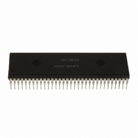
HD6473258P10 Renesas Electronics America, HD6473258P10 Datasheet - Page 55

HD6473258P10
Manufacturer Part Number
HD6473258P10
Description
IC H8 MCU OTP 32K 64DIP
Manufacturer
Renesas Electronics America
Series
H8® H8/325r
Datasheet
1.HD6413238F10.pdf
(301 pages)
Specifications of HD6473258P10
Core Processor
H8/300
Core Size
8-Bit
Speed
10MHz
Connectivity
SCI, UART/USART
Number Of I /o
53
Program Memory Size
32KB (32K x 8)
Program Memory Type
OTP
Ram Size
1K x 8
Voltage - Supply (vcc/vdd)
4.5 V ~ 5.5 V
Oscillator Type
External
Operating Temperature
-20°C ~ 75°C
Package / Case
64-DIP
Lead Free Status / RoHS Status
Contains lead / RoHS non-compliant
Eeprom Size
-
Data Converters
-
Peripherals
-
Available stocks
Company
Part Number
Manufacturer
Quantity
Price
Company:
Part Number:
HD6473258P10
Manufacturer:
EXEL
Quantity:
6 218
Company:
Part Number:
HD6473258P10V
Manufacturer:
RENESAS
Quantity:
600
Part Number:
HD6473258P10V
Manufacturer:
HITACHI/日立
Quantity:
20 000
- Current page: 55 of 301
- Download datasheet (2Mb)
Before Execution of BSET Instruction
Input/output
Pin state
DDR
DR
Pull-up Mos
Execution of BSET Instruction
BSET.B
After Execution of BSET Instruction
Input/output
Pin state
DDR
DR
Pull-up
Explanation: To execute the BSET instruction, the CPU begins by reading port 4. Since P4
P4
It reads P4
Since P4
The CPU therefore reads the value of port 4 as H'40, although the actual value in P4DR is H'80.
Next the CPU sets bit 0 of the read data to "1," changing the value to H'41.
Finally, the CPU writes this value (H'41) back to P4DR to complete the BSET instruction.
As a result, bit P4
both modified, changing the on/off settings of the MOS pull-up transistors of pins P4
Programming Solution: The switching of the pull-ups for P4
avoided by reserving a byte in RAM as a temporary register for P4DR and using it as follows.
RAM0 is a symbol for the user-selected address of the temporary register.
6
are input pins, the CPU reads the level of these pins directly, not the value in the data register.
5
#0, @PORT4
to P4
7
as Low ("0") and P4
0
are output pins, for these pins the CPU reads the value in the data register ("0").
P4
Input
Low
0
1
On
P4
Input
Low
0
0
Off
0
is set to "1," switching pin P4
7
7
P4
Input
High
0
0
Off
P4
Input
High
0
1
On
6
6
;set bit 0 in data register
6
as High ("1").
P4
Output Output Output Output Output Output
Low
1
0
Off
P4
Output Output Output Output Output Output
Low
1
0
Off
5
5
P4
Low
1
0
Off
P4
Low
1
0
Off
4
4
46
0
to High output. In addition, bits P4
P4
Low
1
0
Off
P4
Low
1
0
Off
3
3
P4
Low
1
0
Off
P4
Low
1
0
Off
7
and P4
2
2
P4
Low
1
0
Off
P4
Low
1
0
Off
6
in example 2 can be
1
1
P4
Low
1
0
Off
P4
High
1
1
Off
0
0
7
7
and P4
and P4
7
6
.
6
and
are
Related parts for HD6473258P10
Image
Part Number
Description
Manufacturer
Datasheet
Request
R

Part Number:
Description:
KIT STARTER FOR M16C/29
Manufacturer:
Renesas Electronics America
Datasheet:

Part Number:
Description:
KIT STARTER FOR R8C/2D
Manufacturer:
Renesas Electronics America
Datasheet:

Part Number:
Description:
R0K33062P STARTER KIT
Manufacturer:
Renesas Electronics America
Datasheet:

Part Number:
Description:
KIT STARTER FOR R8C/23 E8A
Manufacturer:
Renesas Electronics America
Datasheet:

Part Number:
Description:
KIT STARTER FOR R8C/25
Manufacturer:
Renesas Electronics America
Datasheet:

Part Number:
Description:
KIT STARTER H8S2456 SHARPE DSPLY
Manufacturer:
Renesas Electronics America
Datasheet:

Part Number:
Description:
KIT STARTER FOR R8C38C
Manufacturer:
Renesas Electronics America
Datasheet:

Part Number:
Description:
KIT STARTER FOR R8C35C
Manufacturer:
Renesas Electronics America
Datasheet:

Part Number:
Description:
KIT STARTER FOR R8CL3AC+LCD APPS
Manufacturer:
Renesas Electronics America
Datasheet:

Part Number:
Description:
KIT STARTER FOR RX610
Manufacturer:
Renesas Electronics America
Datasheet:

Part Number:
Description:
KIT STARTER FOR R32C/118
Manufacturer:
Renesas Electronics America
Datasheet:

Part Number:
Description:
KIT DEV RSK-R8C/26-29
Manufacturer:
Renesas Electronics America
Datasheet:

Part Number:
Description:
KIT STARTER FOR SH7124
Manufacturer:
Renesas Electronics America
Datasheet:

Part Number:
Description:
KIT STARTER FOR H8SX/1622
Manufacturer:
Renesas Electronics America
Datasheet:

Part Number:
Description:
KIT DEV FOR SH7203
Manufacturer:
Renesas Electronics America
Datasheet:


