HD6473258P10 Renesas Electronics America, HD6473258P10 Datasheet - Page 6
HD6473258P10
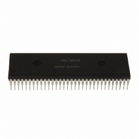
Manufacturer Part Number
HD6473258P10
Description
IC H8 MCU OTP 32K 64DIP
Manufacturer
Renesas Electronics America
Series
H8® H8/325r
Datasheet
1.HD6413238F10.pdf
(301 pages)
Specifications of HD6473258P10
Core Processor
H8/300
Core Size
8-Bit
Speed
10MHz
Connectivity
SCI, UART/USART
Number Of I /o
53
Program Memory Size
32KB (32K x 8)
Program Memory Type
OTP
Ram Size
1K x 8
Voltage - Supply (vcc/vdd)
4.5 V ~ 5.5 V
Oscillator Type
External
Operating Temperature
-20°C ~ 75°C
Package / Case
64-DIP
Lead Free Status / RoHS Status
Contains lead / RoHS non-compliant
Eeprom Size
-
Data Converters
-
Peripherals
-
Available stocks
Company
Part Number
Manufacturer
Quantity
Price
Company:

Part Number:
HD6473258P10
Manufacturer:
EXEL
Quantity:
6 218
Company:
Part Number:
HD6473258P10V
Manufacturer:
RENESAS
Quantity:
600
Part Number:
HD6473258P10V
Manufacturer:
HITACHI/日立
Quantity:
20 000


Section 6. Parallel Handshaking Interface
6.1
6.2
6.3
Section 7. 16-Bit Free-Running Timer
7.1
7.2
7.3
7.4
Overview............................................................................................................................... 113
6.1.1
6.1.2
6.1.3
6.1.4
Register Descriptions............................................................................................................ 115
6.2.1
6.2.2
6.2.3
Operation .............................................................................................................................. 118
6.3.1
6.3.2
6.3.3
6.3.4
6.3.5
Overview............................................................................................................................... 123
7.1.1
7.1.2
7.1.3
7.1.4
Register Descriptions............................................................................................................ 126
7.2.1
7.2.2
7.2.3
7.2.4
7.2.5
7.2.6
CPU Interface ....................................................................................................................... 133
Operation .............................................................................................................................. 136
7.4.1
7.4.2
7.4.3
7.4.4
7.4.5
Features.................................................................................................................... 113
Block Diagram......................................................................................................... 114
Input and Output Pins .............................................................................................. 115
Register Configuration ............................................................................................ 115
Port 3 Data Direction Register (P3DDR) ................................................................ 115
Port 3 Data Register (P3DR) ................................................................................... 116
Handshake Control/Status Register (HCSR)........................................................... 116
Output Timing of Output Strobe Signal .................................................................. 118
Busy Signal Output Timing ..................................................................................... 119
Operation in Software Standby Mode ..................................................................... 119
Sample Application ................................................................................................. 120
Interrupts.................................................................................................................. 121
Features.................................................................................................................... 123
Block Diagram......................................................................................................... 123
Input and Output Pins .............................................................................................. 125
Register Configuration ............................................................................................ 125
Free-Running Counter (FRC) – H’FF92 ................................................................. 126
Output Compare Registers A and B
(OCRA and OCRB) – H’FF94 and H’FF96............................................................ 126
Input Capture Register (ICR) – H’FF98.................................................................. 127
Timer Control Register (TCR) – H’FF90................................................................ 128
Timer Control/Status Register (TCSR) – H’FF91................................................... 130
FRT Noise Canceler Control Register (FNCR) – H’FFFF...................................... 133
FRC Incrementation Timing.................................................................................... 136
Output Compare Timing.......................................................................................... 138
FRC Clear Timing ................................................................................................... 138
Input Capture Timing .............................................................................................. 139
Timing of Input Capture Flag (ICF) Setting............................................................ 140
.............................................................................. 123
iii
....................................................................... 113
Related parts for HD6473258P10
Image
Part Number
Description
Manufacturer
Datasheet
Request
R

Part Number:
Description:
KIT STARTER FOR M16C/29
Manufacturer:
Renesas Electronics America
Datasheet:

Part Number:
Description:
KIT STARTER FOR R8C/2D
Manufacturer:
Renesas Electronics America
Datasheet:

Part Number:
Description:
R0K33062P STARTER KIT
Manufacturer:
Renesas Electronics America
Datasheet:

Part Number:
Description:
KIT STARTER FOR R8C/23 E8A
Manufacturer:
Renesas Electronics America
Datasheet:

Part Number:
Description:
KIT STARTER FOR R8C/25
Manufacturer:
Renesas Electronics America
Datasheet:

Part Number:
Description:
KIT STARTER H8S2456 SHARPE DSPLY
Manufacturer:
Renesas Electronics America
Datasheet:

Part Number:
Description:
KIT STARTER FOR R8C38C
Manufacturer:
Renesas Electronics America
Datasheet:

Part Number:
Description:
KIT STARTER FOR R8C35C
Manufacturer:
Renesas Electronics America
Datasheet:

Part Number:
Description:
KIT STARTER FOR R8CL3AC+LCD APPS
Manufacturer:
Renesas Electronics America
Datasheet:
Part Number:
Description:
KIT STARTER FOR RX610
Manufacturer:
Renesas Electronics America
Datasheet:

Part Number:
Description:
KIT STARTER FOR R32C/118
Manufacturer:
Renesas Electronics America
Datasheet:

Part Number:
Description:
KIT DEV RSK-R8C/26-29
Manufacturer:
Renesas Electronics America
Datasheet:

Part Number:
Description:
KIT STARTER FOR SH7124
Manufacturer:
Renesas Electronics America
Datasheet:

Part Number:
Description:
KIT STARTER FOR H8SX/1622
Manufacturer:
Renesas Electronics America
Datasheet:

Part Number:
Description:
KIT DEV FOR SH7203
Manufacturer:
Renesas Electronics America
Datasheet: