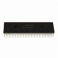
HD6473258P10 Renesas Electronics America, HD6473258P10 Datasheet - Page 104

HD6473258P10
Manufacturer Part Number
HD6473258P10
Description
IC H8 MCU OTP 32K 64DIP
Manufacturer
Renesas Electronics America
Series
H8® H8/325r
Datasheet
1.HD6413238F10.pdf
(301 pages)
Specifications of HD6473258P10
Core Processor
H8/300
Core Size
8-Bit
Speed
10MHz
Connectivity
SCI, UART/USART
Number Of I /o
53
Program Memory Size
32KB (32K x 8)
Program Memory Type
OTP
Ram Size
1K x 8
Voltage - Supply (vcc/vdd)
4.5 V ~ 5.5 V
Oscillator Type
External
Operating Temperature
-20°C ~ 75°C
Package / Case
64-DIP
Lead Free Status / RoHS Status
Contains lead / RoHS non-compliant
Eeprom Size
-
Data Converters
-
Peripherals
-
Available stocks
Company
Part Number
Manufacturer
Quantity
Price
Company:
Part Number:
HD6473258P10
Manufacturer:
EXEL
Quantity:
6 218
Company:
Part Number:
HD6473258P10V
Manufacturer:
RENESAS
Quantity:
600
Part Number:
HD6473258P10V
Manufacturer:
HITACHI/日立
Quantity:
20 000
- Current page: 104 of 301
- Download datasheet (2Mb)
See section 9, Serial Communication Interface for details of the serial control bits. Pins used by the
serial communication interface are switched between input and output without regard to the values
in the data direction register.
Pins of port 5 can drive a single TTL load and a 30-pF capacitive load when they are used as output
pins. They can also drive a Darlington pair.
Table 5-11 details the port 5 registers.
Table 5-11. Port 5 Registers
Name
Port 5 data direction register
Port 5 data register
Port 5 Data Direction Register (P5DDR)—H’FFB8
Bit
Initial value
Read/Write
P5DDR is an 8-bit register that selects the direction of each pin in port 5. A pin functions as an
output pin if the corresponding bit in P5DDR is set to 1, and as an input pin if the bit is cleared to 0.
Port 5 Data Register (P5DR)—H’FFBA
Bit
Initial value
Read/Write
P5DR is an 8-bit register containing output data for pins P5
ups. When the CPU reads P5DR, for output pins (P5DDR = 1) it reads the value in the P5DR latch,
but for input pins (P5DDR = 0), it obtains the logic level directly from the pin, bypassing the P5DR
latch. This also applies to pins used for serial communication.
MOS Pull-Ups: Are available for input pins, including serial communication input pins. Software
can turn the MOS pull-up on by writing a 1 in P5DR, and turn it off by writing a 0. The pull-ups are
automatically turned off for output pins.
—
—
—
—
7
1
7
1
—
—
—
—
6
1
6
1
Abbreviation
P5DDR
P5DR
P5
R/W
5
P5
W
DDR P5
5
0
5
0
5
R/W
95
Read/Write
W
R/W
4
P5
W
DDR P5
4
0
4
0
4
R/W
3
P5
5
W
DDR P5
3
0
3
0
to P5
3
Initial value
H’C0
H’C0
0
, and controlling their input pull-
R/W
2
P5
W
DDR P5
2
0
2
0
2
R/W
1
P5
W
DDR P5
1
0
1
0
1
R/W
0
P5
W
DDR
0
0
0
0
Address
H’FFB8
H’FFBA
0
Related parts for HD6473258P10
Image
Part Number
Description
Manufacturer
Datasheet
Request
R

Part Number:
Description:
KIT STARTER FOR M16C/29
Manufacturer:
Renesas Electronics America
Datasheet:

Part Number:
Description:
KIT STARTER FOR R8C/2D
Manufacturer:
Renesas Electronics America
Datasheet:

Part Number:
Description:
R0K33062P STARTER KIT
Manufacturer:
Renesas Electronics America
Datasheet:

Part Number:
Description:
KIT STARTER FOR R8C/23 E8A
Manufacturer:
Renesas Electronics America
Datasheet:

Part Number:
Description:
KIT STARTER FOR R8C/25
Manufacturer:
Renesas Electronics America
Datasheet:

Part Number:
Description:
KIT STARTER H8S2456 SHARPE DSPLY
Manufacturer:
Renesas Electronics America
Datasheet:

Part Number:
Description:
KIT STARTER FOR R8C38C
Manufacturer:
Renesas Electronics America
Datasheet:

Part Number:
Description:
KIT STARTER FOR R8C35C
Manufacturer:
Renesas Electronics America
Datasheet:

Part Number:
Description:
KIT STARTER FOR R8CL3AC+LCD APPS
Manufacturer:
Renesas Electronics America
Datasheet:

Part Number:
Description:
KIT STARTER FOR RX610
Manufacturer:
Renesas Electronics America
Datasheet:

Part Number:
Description:
KIT STARTER FOR R32C/118
Manufacturer:
Renesas Electronics America
Datasheet:

Part Number:
Description:
KIT DEV RSK-R8C/26-29
Manufacturer:
Renesas Electronics America
Datasheet:

Part Number:
Description:
KIT STARTER FOR SH7124
Manufacturer:
Renesas Electronics America
Datasheet:

Part Number:
Description:
KIT STARTER FOR H8SX/1622
Manufacturer:
Renesas Electronics America
Datasheet:

Part Number:
Description:
KIT DEV FOR SH7203
Manufacturer:
Renesas Electronics America
Datasheet:


