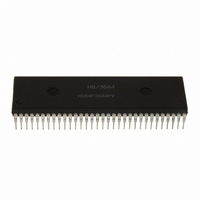
HD6473258P10 Renesas Electronics America, HD6473258P10 Datasheet - Page 198

HD6473258P10
Manufacturer Part Number
HD6473258P10
Description
IC H8 MCU OTP 32K 64DIP
Manufacturer
Renesas Electronics America
Series
H8® H8/325r
Datasheet
1.HD6413238F10.pdf
(301 pages)
Specifications of HD6473258P10
Core Processor
H8/300
Core Size
8-Bit
Speed
10MHz
Connectivity
SCI, UART/USART
Number Of I /o
53
Program Memory Size
32KB (32K x 8)
Program Memory Type
OTP
Ram Size
1K x 8
Voltage - Supply (vcc/vdd)
4.5 V ~ 5.5 V
Oscillator Type
External
Operating Temperature
-20°C ~ 75°C
Package / Case
64-DIP
Lead Free Status / RoHS Status
Contains lead / RoHS non-compliant
Eeprom Size
-
Data Converters
-
Peripherals
-
Available stocks
Company
Part Number
Manufacturer
Quantity
Price
Company:
Part Number:
HD6473258P10
Manufacturer:
EXEL
Quantity:
6 218
Company:
Part Number:
HD6473258P10V
Manufacturer:
RENESAS
Quantity:
600
Part Number:
HD6473258P10V
Manufacturer:
HITACHI/日立
Quantity:
20 000
- Current page: 198 of 301
- Download datasheet (2Mb)
The RDR and RSR function as a double buffer. Data can be received continuously by reading each
byte of data from the RDR and clearing the RDRF bit to 0 before the last bit of the next byte is
received.
In general, an external clock source should be used for receiving data.
If an internal clock source is selected, the SCI starts receiving data as soon as the RE bit is set to 1.
The serial clock is also output at the SCK pin. The SCI continues receiving until the RE bit is
cleared to 0.
If the last bit of the next data byte is received while the RDRF bit is still set to 1, an overrun error
occurs and the ORER bit is set to 1. If the RIE bit is set to 1, a receive-error interrupt (ERI) is
requested. The data received in the RSR are not transferred to the RDR when an overrun error
occurs.
After an overrun error, reception of the next data is enabled when the ORER bit is cleared to 0.
• Simultaneous Transmit and Receive: The procedure for transmitting and receiving
simultaneously is as follows:
Set up the desired receiving conditions in the SMR, BRR, and SCR.
Set the RE bit in the SCR to 1.
The RxD pin is automatically be switched to input and the SCI is ready to receive data.
Incoming data bits are latched in the RSR on eight clock pulses.
When 8 bits of data have been received, the SCI sets the RDRF bit in the SSR to 1. If the RIE
bit is set to 1, a receive-end interrupt (RXI) is requested.
The SCI transfers the received data byte from the RSR to the RDR so that it can be read.
The RDRF bit is cleared when software reads the RDRF bit in the SSR, then writes a 0 in the
RDRF bit.
Set up the desired communication conditions in the SMR, BRR, and SCR.
Set the TE and RE bits in the SCR to 1.
The TxD and RxD pins are automatically switched to output and input, respectively, and the
SCI is ready to transmit and receive data.
191
Related parts for HD6473258P10
Image
Part Number
Description
Manufacturer
Datasheet
Request
R

Part Number:
Description:
KIT STARTER FOR M16C/29
Manufacturer:
Renesas Electronics America
Datasheet:

Part Number:
Description:
KIT STARTER FOR R8C/2D
Manufacturer:
Renesas Electronics America
Datasheet:

Part Number:
Description:
R0K33062P STARTER KIT
Manufacturer:
Renesas Electronics America
Datasheet:

Part Number:
Description:
KIT STARTER FOR R8C/23 E8A
Manufacturer:
Renesas Electronics America
Datasheet:

Part Number:
Description:
KIT STARTER FOR R8C/25
Manufacturer:
Renesas Electronics America
Datasheet:

Part Number:
Description:
KIT STARTER H8S2456 SHARPE DSPLY
Manufacturer:
Renesas Electronics America
Datasheet:

Part Number:
Description:
KIT STARTER FOR R8C38C
Manufacturer:
Renesas Electronics America
Datasheet:

Part Number:
Description:
KIT STARTER FOR R8C35C
Manufacturer:
Renesas Electronics America
Datasheet:

Part Number:
Description:
KIT STARTER FOR R8CL3AC+LCD APPS
Manufacturer:
Renesas Electronics America
Datasheet:

Part Number:
Description:
KIT STARTER FOR RX610
Manufacturer:
Renesas Electronics America
Datasheet:

Part Number:
Description:
KIT STARTER FOR R32C/118
Manufacturer:
Renesas Electronics America
Datasheet:

Part Number:
Description:
KIT DEV RSK-R8C/26-29
Manufacturer:
Renesas Electronics America
Datasheet:

Part Number:
Description:
KIT STARTER FOR SH7124
Manufacturer:
Renesas Electronics America
Datasheet:

Part Number:
Description:
KIT STARTER FOR H8SX/1622
Manufacturer:
Renesas Electronics America
Datasheet:

Part Number:
Description:
KIT DEV FOR SH7203
Manufacturer:
Renesas Electronics America
Datasheet:


