HD6473258P10 Renesas Electronics America, HD6473258P10 Datasheet - Page 262
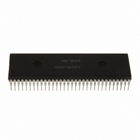
HD6473258P10
Manufacturer Part Number
HD6473258P10
Description
IC H8 MCU OTP 32K 64DIP
Manufacturer
Renesas Electronics America
Series
H8® H8/325r
Datasheet
1.HD6413238F10.pdf
(301 pages)
Specifications of HD6473258P10
Core Processor
H8/300
Core Size
8-Bit
Speed
10MHz
Connectivity
SCI, UART/USART
Number Of I /o
53
Program Memory Size
32KB (32K x 8)
Program Memory Type
OTP
Ram Size
1K x 8
Voltage - Supply (vcc/vdd)
4.5 V ~ 5.5 V
Oscillator Type
External
Operating Temperature
-20°C ~ 75°C
Package / Case
64-DIP
Lead Free Status / RoHS Status
Contains lead / RoHS non-compliant
Eeprom Size
-
Data Converters
-
Peripherals
-
Available stocks
Company
Part Number
Manufacturer
Quantity
Price
Company:

Part Number:
HD6473258P10
Manufacturer:
EXEL
Quantity:
6 218
Company:
Part Number:
HD6473258P10V
Manufacturer:
RENESAS
Quantity:
600
Part Number:
HD6473258P10V
Manufacturer:
HITACHI/日立
Quantity:
20 000


A.3 Number of States Required for Execution
The tables below can be used to calculate the number of states required for instruction execution.
Table A-3 indicates the number of states required for each cycle (instruction fetch, branch address
read, stack operation, byte data access, word data access, internal operation). Table A-4 indicates
the number of cycles of each type occurring in each instruction. The total number of states required
for execution of an instruction can be calculated from these two tables as follows:
Execution states = I S
Examples: Mode 1 (on-chip ROM disabled), stack located in external memory, 1 wait state
inserted in external memory access.
1. BSET #0, @FFC7
2. JSR @@30
Table A-3. Number of States Taken by Each Cycle in Instruction Execution
Execution status
(instruction cycle)
Instruction fetch
Branch address read S
Stack operation
Byte data access
Word data access
Internal operation
Notes: 1. m: Number of wait states inserted in access to external device.
From table A-4: I = L = 2,
From table A-3: S
Number of states required for execution: 2 8 + 2 3 =22
From table A-4: I = 2,
From table A-3: S
Number of states required for execution: 2 8 + 1 8 + 1 8 = 32
2. The byte data access cycle to an external device by the MOVFPE and MOVTPE
instructions requires 9 to 16 states since it is synchronized with the E clock. See
section 13, E-Clock Interface for timing details.
S
S
S
S
S
I
I
I
J
K
L
M
N
I
= 8,
= S
+ J S
J
= S
J = K = 1,
S
J
K
2
On-chip memory
L
+ K S
J = K = M = N= 0
= 3
= 8
K
L = M = N = 0
+ L S
266
L
Access location
+ M S
On-chip reg. field
6
3
6
2
M
+ N S
N
External memory
6 + 2m
3 + m (note 2)
6 + 2m
Related parts for HD6473258P10
Image
Part Number
Description
Manufacturer
Datasheet
Request
R

Part Number:
Description:
KIT STARTER FOR M16C/29
Manufacturer:
Renesas Electronics America
Datasheet:

Part Number:
Description:
KIT STARTER FOR R8C/2D
Manufacturer:
Renesas Electronics America
Datasheet:

Part Number:
Description:
R0K33062P STARTER KIT
Manufacturer:
Renesas Electronics America
Datasheet:

Part Number:
Description:
KIT STARTER FOR R8C/23 E8A
Manufacturer:
Renesas Electronics America
Datasheet:

Part Number:
Description:
KIT STARTER FOR R8C/25
Manufacturer:
Renesas Electronics America
Datasheet:

Part Number:
Description:
KIT STARTER H8S2456 SHARPE DSPLY
Manufacturer:
Renesas Electronics America
Datasheet:

Part Number:
Description:
KIT STARTER FOR R8C38C
Manufacturer:
Renesas Electronics America
Datasheet:

Part Number:
Description:
KIT STARTER FOR R8C35C
Manufacturer:
Renesas Electronics America
Datasheet:

Part Number:
Description:
KIT STARTER FOR R8CL3AC+LCD APPS
Manufacturer:
Renesas Electronics America
Datasheet:
Part Number:
Description:
KIT STARTER FOR RX610
Manufacturer:
Renesas Electronics America
Datasheet:

Part Number:
Description:
KIT STARTER FOR R32C/118
Manufacturer:
Renesas Electronics America
Datasheet:

Part Number:
Description:
KIT DEV RSK-R8C/26-29
Manufacturer:
Renesas Electronics America
Datasheet:

Part Number:
Description:
KIT STARTER FOR SH7124
Manufacturer:
Renesas Electronics America
Datasheet:

Part Number:
Description:
KIT STARTER FOR H8SX/1622
Manufacturer:
Renesas Electronics America
Datasheet:

Part Number:
Description:
KIT DEV FOR SH7203
Manufacturer:
Renesas Electronics America
Datasheet: