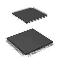
DF2166VT33WV Renesas Electronics America, DF2166VT33WV Datasheet - Page 834

DF2166VT33WV
Manufacturer Part Number
DF2166VT33WV
Description
MCU 16BIT FLASH 3V 512K 144-TQFP
Manufacturer
Renesas Electronics America
Series
H8® H8S/2100r
Datasheet
1.HS2168EPI61H-U.pdf
(876 pages)
Specifications of DF2166VT33WV
Core Processor
H8S/2000
Core Size
16-Bit
Speed
33MHz
Connectivity
I²C, IrDA, LPC, SCI, SmartCard
Peripherals
POR, PWM, WDT
Number Of I /o
106
Program Memory Size
512KB (512K x 8)
Program Memory Type
FLASH
Ram Size
40K x 8
Voltage - Supply (vcc/vdd)
3 V ~ 3.6 V
Data Converters
A/D 8x10b; D/A 2x8b
Oscillator Type
External
Operating Temperature
-20°C ~ 75°C
Package / Case
144-TQFP, 144-VQFP
Lead Free Status / RoHS Status
Lead free / RoHS Compliant
Eeprom Size
-
Available stocks
Company
Part Number
Manufacturer
Quantity
Price
Company:
Part Number:
DF2166VT33WV
Manufacturer:
Renesas Electronics America
Quantity:
135
Company:
Part Number:
DF2166VT33WV
Manufacturer:
Renesas Electronics America
Quantity:
10 000
- Current page: 834 of 876
- Download datasheet (5Mb)
25.3.2
Table 25.7 shows the control signal timing. Only external interrupts NMI, IRQ0 to IRQ15, KIN0
to KIN15, and WUE8 to WUE15 can be operated based on the subclock (φSUB = 32.768 kHz).
Table 25.7 Control Signal Timing
Condition: VCC = 3.0 V to 3.6 V, VSS = 0 V, φ = 5 MHz to 33 MHz
Rev. 3.00, 03/04, page 792 of 830
Item
RES setup time
RES pulse width
NMI setup time
NMI hold time
NMI pulse width
(exiting software standby
mode)
IRQ setup time
(IRQ15 to IRQ0, KIN15
to KIN0, WUE15 to
WUE8)
IRQ hold time
(IRQ15 to IRQ0, KIN15
to KIN0, WUE15 to
WUE8)
IRQ pulse width
(IRQ15 to IRQ0, KIN15
to KIN0, WUE15 to
WUE8) (exiting software
standby mode)
Control Signal Timing
RES
φ
Symbol
t
t
t
t
t
t
t
t
RESS
RESW
NMIS
NMIH
NMIW
IRQS
IRQH
IRQW
Figure 25.10 Reset Input Timing
Min.
200
20
150
10
200
150
10
200
t
RESS
Max.
t
RESW
Unit
ns
t
ns
cyc
t
RESS
Test Conditions
Figure 25.10
Figure 25.11
Related parts for DF2166VT33WV
Image
Part Number
Description
Manufacturer
Datasheet
Request
R

Part Number:
Description:
KIT STARTER FOR M16C/29
Manufacturer:
Renesas Electronics America
Datasheet:

Part Number:
Description:
KIT STARTER FOR R8C/2D
Manufacturer:
Renesas Electronics America
Datasheet:

Part Number:
Description:
R0K33062P STARTER KIT
Manufacturer:
Renesas Electronics America
Datasheet:

Part Number:
Description:
KIT STARTER FOR R8C/23 E8A
Manufacturer:
Renesas Electronics America
Datasheet:

Part Number:
Description:
KIT STARTER FOR R8C/25
Manufacturer:
Renesas Electronics America
Datasheet:

Part Number:
Description:
KIT STARTER H8S2456 SHARPE DSPLY
Manufacturer:
Renesas Electronics America
Datasheet:

Part Number:
Description:
KIT STARTER FOR R8C38C
Manufacturer:
Renesas Electronics America
Datasheet:

Part Number:
Description:
KIT STARTER FOR R8C35C
Manufacturer:
Renesas Electronics America
Datasheet:

Part Number:
Description:
KIT STARTER FOR R8CL3AC+LCD APPS
Manufacturer:
Renesas Electronics America
Datasheet:

Part Number:
Description:
KIT STARTER FOR RX610
Manufacturer:
Renesas Electronics America
Datasheet:

Part Number:
Description:
KIT STARTER FOR R32C/118
Manufacturer:
Renesas Electronics America
Datasheet:

Part Number:
Description:
KIT DEV RSK-R8C/26-29
Manufacturer:
Renesas Electronics America
Datasheet:

Part Number:
Description:
KIT STARTER FOR SH7124
Manufacturer:
Renesas Electronics America
Datasheet:

Part Number:
Description:
KIT STARTER FOR H8SX/1622
Manufacturer:
Renesas Electronics America
Datasheet:

Part Number:
Description:
KIT DEV FOR SH7203
Manufacturer:
Renesas Electronics America
Datasheet:


