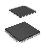
DF2166VT33WV Renesas Electronics America, DF2166VT33WV Datasheet - Page 53

DF2166VT33WV
Manufacturer Part Number
DF2166VT33WV
Description
MCU 16BIT FLASH 3V 512K 144-TQFP
Manufacturer
Renesas Electronics America
Series
H8® H8S/2100r
Datasheet
1.HS2168EPI61H-U.pdf
(876 pages)
Specifications of DF2166VT33WV
Core Processor
H8S/2000
Core Size
16-Bit
Speed
33MHz
Connectivity
I²C, IrDA, LPC, SCI, SmartCard
Peripherals
POR, PWM, WDT
Number Of I /o
106
Program Memory Size
512KB (512K x 8)
Program Memory Type
FLASH
Ram Size
40K x 8
Voltage - Supply (vcc/vdd)
3 V ~ 3.6 V
Data Converters
A/D 8x10b; D/A 2x8b
Oscillator Type
External
Operating Temperature
-20°C ~ 75°C
Package / Case
144-TQFP, 144-VQFP
Lead Free Status / RoHS Status
Lead free / RoHS Compliant
Eeprom Size
-
Available stocks
Company
Part Number
Manufacturer
Quantity
Price
Company:
Part Number:
DF2166VT33WV
Manufacturer:
Renesas Electronics America
Quantity:
135
Company:
Part Number:
DF2166VT33WV
Manufacturer:
Renesas Electronics America
Quantity:
10 000
- Current page: 53 of 876
- Download datasheet (5Mb)
Type
PWM timer
(PWM)
14-bit PWM
timer
(PWMX)
16-bit free
running
timer (FRT)
8-bit timer
(TMR_0,
TMR_1,
TMR_X,
TMR_Y)
Serial
communi-
cation
Interface
(SCI_0,
SCI_1,
SCI_2)
SCI with
IrDA (SCI)
I
interface
(IIC)
2
C bus
PW15 to
PW0
ExPW2 to
ExPW0
PWX0
PWX1
PWX2
PWX3
FTCI
FTOA
FTOB
FTIA to
FTID
TMO0
TMO1
TMOX
TMOY
TMI0
TMI1
TMIX
TMIY
ExTMI0
ExTMI1
ExTMIX
ExTMIY
TxD0 to
TxD2
RxD0 to
RxD2
SCK0 to
SCK2
SSE0I
SSE2I
IrTxD
IrRxD
SCL0 to
SCL5
SDA0 to
SDA5
Symbol
16, 133
136
15, 134
137
46, 45
44
41
40
133
134
50, 48, 32,
30, 28, 60
49, 47, 31,
29, 27, 59
96 to 110
112
92 to 94
5
6
26
25
78
79
84
80 to 83
131
132
3
4
129
130
138
2
46
45
44
43
Pin No.
Output
Input
Input/
Output
Input
Input
Output
Input
Input/
Output
Input/
Output
I/O
Output
Output
Input
Output
Input
Output
Input
Transmit data output pins
Receive data input pins
Clock input/output pins. Output format is NMOS
push-pull output.
Input pin to halt SCI_0
Input pin to halt SCI_2
Encoded data output pin for IrDA
Encoded data input pin for IrDA
IIC clock input/output pins. These pins can drive a
bus directly with the NMOS open drain output.
IIC data input/output pins. These pins can drive a
bus directly with the NMOS open drain output.
Name and Function
PWM timer pulse output pins.
Selectable from which pin of PWn or ExPWn to
output PW2 to PW0.
PWM D/A pulse output pins
External event input pin
Output compare output pins
Input capture input pins
Waveform output pins with output compare
function
External event input pins and counter reset input
pins. Selectable to which pin of TMIn or ExTMIn
to insert external event and counter reset.
Rev. 3.00, 03/04, page 11 of 830
Related parts for DF2166VT33WV
Image
Part Number
Description
Manufacturer
Datasheet
Request
R

Part Number:
Description:
KIT STARTER FOR M16C/29
Manufacturer:
Renesas Electronics America
Datasheet:

Part Number:
Description:
KIT STARTER FOR R8C/2D
Manufacturer:
Renesas Electronics America
Datasheet:

Part Number:
Description:
R0K33062P STARTER KIT
Manufacturer:
Renesas Electronics America
Datasheet:

Part Number:
Description:
KIT STARTER FOR R8C/23 E8A
Manufacturer:
Renesas Electronics America
Datasheet:

Part Number:
Description:
KIT STARTER FOR R8C/25
Manufacturer:
Renesas Electronics America
Datasheet:

Part Number:
Description:
KIT STARTER H8S2456 SHARPE DSPLY
Manufacturer:
Renesas Electronics America
Datasheet:

Part Number:
Description:
KIT STARTER FOR R8C38C
Manufacturer:
Renesas Electronics America
Datasheet:

Part Number:
Description:
KIT STARTER FOR R8C35C
Manufacturer:
Renesas Electronics America
Datasheet:

Part Number:
Description:
KIT STARTER FOR R8CL3AC+LCD APPS
Manufacturer:
Renesas Electronics America
Datasheet:

Part Number:
Description:
KIT STARTER FOR RX610
Manufacturer:
Renesas Electronics America
Datasheet:

Part Number:
Description:
KIT STARTER FOR R32C/118
Manufacturer:
Renesas Electronics America
Datasheet:

Part Number:
Description:
KIT DEV RSK-R8C/26-29
Manufacturer:
Renesas Electronics America
Datasheet:

Part Number:
Description:
KIT STARTER FOR SH7124
Manufacturer:
Renesas Electronics America
Datasheet:

Part Number:
Description:
KIT STARTER FOR H8SX/1622
Manufacturer:
Renesas Electronics America
Datasheet:

Part Number:
Description:
KIT DEV FOR SH7203
Manufacturer:
Renesas Electronics America
Datasheet:


