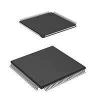
DF2166VT33WV Renesas Electronics America, DF2166VT33WV Datasheet - Page 514

DF2166VT33WV
Manufacturer Part Number
DF2166VT33WV
Description
MCU 16BIT FLASH 3V 512K 144-TQFP
Manufacturer
Renesas Electronics America
Series
H8® H8S/2100r
Datasheet
1.HS2168EPI61H-U.pdf
(876 pages)
Specifications of DF2166VT33WV
Core Processor
H8S/2000
Core Size
16-Bit
Speed
33MHz
Connectivity
I²C, IrDA, LPC, SCI, SmartCard
Peripherals
POR, PWM, WDT
Number Of I /o
106
Program Memory Size
512KB (512K x 8)
Program Memory Type
FLASH
Ram Size
40K x 8
Voltage - Supply (vcc/vdd)
3 V ~ 3.6 V
Data Converters
A/D 8x10b; D/A 2x8b
Oscillator Type
External
Operating Temperature
-20°C ~ 75°C
Package / Case
144-TQFP, 144-VQFP
Lead Free Status / RoHS Status
Lead free / RoHS Compliant
Eeprom Size
-
Available stocks
Company
Part Number
Manufacturer
Quantity
Price
Company:
Part Number:
DF2166VT33WV
Manufacturer:
Renesas Electronics America
Quantity:
135
Company:
Part Number:
DF2166VT33WV
Manufacturer:
Renesas Electronics America
Quantity:
10 000
- Current page: 514 of 876
- Download datasheet (5Mb)
The reception procedure and operations by which the data reception process is provided in 1-byte
units with SCL fixed low at each data reception are described below.
[1]
[2]
[3]
[4]
[5]
[6]
[7]
[8]
[9]
[10]
[11]
Rev. 3.00, 03/04, page 472 of 830
Clear the TRS bit in ICCR to 0 to switch from transmit mode to receive mode.
Clear the ACKB bit in ICSR to 0 (acknowledge data setting).
Set the HNDS bit in ICXR to 1.
Clear the IRIC flag to 0 to determine the end of reception.
Go to step [6] to halt reception operation if the first frame is the last receive data.
When ICDR is read (dummy data read), reception is started, and the receive clock is output,
and data received, in synchronization with the internal clock. (Data from the SDA pin is
sequentially transferred to ICDRS in synchronization with the rise of the receive clock
pulses.)
The master device drives SDA low to return the acknowledge data at the 9th receive clock
pulse. The receive data is transferred to ICDRR from ICDRS at the rise of the 9th clock
pulse, setting the ICDRF, IRIC, and IRTR flags to 1. If the IEIC bit has been set to 1, an
interrupt request is sent to the CPU.
The master device drives SCL low from the fall of the 9th receive clock pulse to the ICDR
data reading.
Clear the IRIC flag to determine the next interrupt.
Go to step [6] to halt reception operation if the next frame is the last receive data.
Read ICDR receive data. This clears the ICDRF flag to 0. The master device outputs the
receive clock continuously to receive the next data.
Data can be received continuously by repeating steps [3] to [5].
Set the ACKB bit to 1 so as to return the acknowledge data for the last reception.
Read ICDR receive data. This clears the ICDRF flag to 0. The master device outputs the
receive clock to receive data.
When one frame of data has been received, the ICDRF, IRIC, and IRTR flags are set to 1 at
the rise of the 9th receive clock pulse.
Clear the IRIC flag to 0.
Read ICDR receive data after setting the TRS bit. This clears the ICDRF flag to 0.
Clear the BBSY bit and SCP bit to 0 in ICCR. This changes SDA from low to high when
SCL is high, and generates the stop condition.
Related parts for DF2166VT33WV
Image
Part Number
Description
Manufacturer
Datasheet
Request
R

Part Number:
Description:
KIT STARTER FOR M16C/29
Manufacturer:
Renesas Electronics America
Datasheet:

Part Number:
Description:
KIT STARTER FOR R8C/2D
Manufacturer:
Renesas Electronics America
Datasheet:

Part Number:
Description:
R0K33062P STARTER KIT
Manufacturer:
Renesas Electronics America
Datasheet:

Part Number:
Description:
KIT STARTER FOR R8C/23 E8A
Manufacturer:
Renesas Electronics America
Datasheet:

Part Number:
Description:
KIT STARTER FOR R8C/25
Manufacturer:
Renesas Electronics America
Datasheet:

Part Number:
Description:
KIT STARTER H8S2456 SHARPE DSPLY
Manufacturer:
Renesas Electronics America
Datasheet:

Part Number:
Description:
KIT STARTER FOR R8C38C
Manufacturer:
Renesas Electronics America
Datasheet:

Part Number:
Description:
KIT STARTER FOR R8C35C
Manufacturer:
Renesas Electronics America
Datasheet:

Part Number:
Description:
KIT STARTER FOR R8CL3AC+LCD APPS
Manufacturer:
Renesas Electronics America
Datasheet:

Part Number:
Description:
KIT STARTER FOR RX610
Manufacturer:
Renesas Electronics America
Datasheet:

Part Number:
Description:
KIT STARTER FOR R32C/118
Manufacturer:
Renesas Electronics America
Datasheet:

Part Number:
Description:
KIT DEV RSK-R8C/26-29
Manufacturer:
Renesas Electronics America
Datasheet:

Part Number:
Description:
KIT STARTER FOR SH7124
Manufacturer:
Renesas Electronics America
Datasheet:

Part Number:
Description:
KIT STARTER FOR H8SX/1622
Manufacturer:
Renesas Electronics America
Datasheet:

Part Number:
Description:
KIT DEV FOR SH7203
Manufacturer:
Renesas Electronics America
Datasheet:


