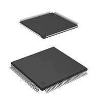
DF2166VT33WV Renesas Electronics America, DF2166VT33WV Datasheet - Page 146

DF2166VT33WV
Manufacturer Part Number
DF2166VT33WV
Description
MCU 16BIT FLASH 3V 512K 144-TQFP
Manufacturer
Renesas Electronics America
Series
H8® H8S/2100r
Datasheet
1.HS2168EPI61H-U.pdf
(876 pages)
Specifications of DF2166VT33WV
Core Processor
H8S/2000
Core Size
16-Bit
Speed
33MHz
Connectivity
I²C, IrDA, LPC, SCI, SmartCard
Peripherals
POR, PWM, WDT
Number Of I /o
106
Program Memory Size
512KB (512K x 8)
Program Memory Type
FLASH
Ram Size
40K x 8
Voltage - Supply (vcc/vdd)
3 V ~ 3.6 V
Data Converters
A/D 8x10b; D/A 2x8b
Oscillator Type
External
Operating Temperature
-20°C ~ 75°C
Package / Case
144-TQFP, 144-VQFP
Lead Free Status / RoHS Status
Lead free / RoHS Compliant
Eeprom Size
-
Available stocks
Company
Part Number
Manufacturer
Quantity
Price
Company:
Part Number:
DF2166VT33WV
Manufacturer:
Renesas Electronics America
Quantity:
135
Company:
Part Number:
DF2166VT33WV
Manufacturer:
Renesas Electronics America
Quantity:
10 000
- Current page: 146 of 876
- Download datasheet (5Mb)
6.2
Table 6.1 summarizes the pin configuration of the bus controller.
Table 6.1
Rev. 3.00, 03/04, page 104 of 830
Symbol
AS
IOS
CPCS1
CS256
RD
HWR
LWR
WAIT
AH
AD15 to AD0
Input/Output Pins
Pin Configuration
Output
Output
Output
Output
Output
Output
Output
Input
Output
I/O
Input/Output
Function
Strobe signal indicating that address output on the address
bus is enabled (when the IOSE bit in SYSCR is cleared to 0).
Note that this signal is not output when the 256-kbyte
extended area is accessed (the CS256E bit in SYSCR is 1)
or when the CP extended area is accessed (the CPCSE bit
in BCR2 is 1).
Chip select signal indicating that the IOS extended area is
being accessed (when the IOSE bit in SYSCR is 1).
Chip select signal indicating that the CP extended area is
being accessed (when the CPCSE bit in BCR2 is 1).
Chip select signal indicating that the 256-kbyte extended
area is being accessed (when the CS256E bit in SYSCR is
1).
Strobe signal indicating that the external address space is
being read.
Strobe signal indicating that the external address space is
being written to, and the upper half (D15 to D8, AD15 to
AD8) of the data bus is enabled.
Strobe signal indicating that the external address space is
being written to, and the lower half (D7 to D0, AD7 to AD0) of
the data bus is enabled.
Wait request signal when accessing the external space.
Signal indicating address fetch timing when the bus is in
address-data multiplex bus state.
Address output and data input/output pins for address-data
multiplex extension.
Related parts for DF2166VT33WV
Image
Part Number
Description
Manufacturer
Datasheet
Request
R

Part Number:
Description:
KIT STARTER FOR M16C/29
Manufacturer:
Renesas Electronics America
Datasheet:

Part Number:
Description:
KIT STARTER FOR R8C/2D
Manufacturer:
Renesas Electronics America
Datasheet:

Part Number:
Description:
R0K33062P STARTER KIT
Manufacturer:
Renesas Electronics America
Datasheet:

Part Number:
Description:
KIT STARTER FOR R8C/23 E8A
Manufacturer:
Renesas Electronics America
Datasheet:

Part Number:
Description:
KIT STARTER FOR R8C/25
Manufacturer:
Renesas Electronics America
Datasheet:

Part Number:
Description:
KIT STARTER H8S2456 SHARPE DSPLY
Manufacturer:
Renesas Electronics America
Datasheet:

Part Number:
Description:
KIT STARTER FOR R8C38C
Manufacturer:
Renesas Electronics America
Datasheet:

Part Number:
Description:
KIT STARTER FOR R8C35C
Manufacturer:
Renesas Electronics America
Datasheet:

Part Number:
Description:
KIT STARTER FOR R8CL3AC+LCD APPS
Manufacturer:
Renesas Electronics America
Datasheet:

Part Number:
Description:
KIT STARTER FOR RX610
Manufacturer:
Renesas Electronics America
Datasheet:

Part Number:
Description:
KIT STARTER FOR R32C/118
Manufacturer:
Renesas Electronics America
Datasheet:

Part Number:
Description:
KIT DEV RSK-R8C/26-29
Manufacturer:
Renesas Electronics America
Datasheet:

Part Number:
Description:
KIT STARTER FOR SH7124
Manufacturer:
Renesas Electronics America
Datasheet:

Part Number:
Description:
KIT STARTER FOR H8SX/1622
Manufacturer:
Renesas Electronics America
Datasheet:

Part Number:
Description:
KIT DEV FOR SH7203
Manufacturer:
Renesas Electronics America
Datasheet:


