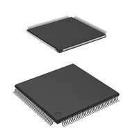
DF2166VT33WV Renesas Electronics America, DF2166VT33WV Datasheet - Page 447

DF2166VT33WV
Manufacturer Part Number
DF2166VT33WV
Description
MCU 16BIT FLASH 3V 512K 144-TQFP
Manufacturer
Renesas Electronics America
Series
H8® H8S/2100r
Datasheet
1.HS2168EPI61H-U.pdf
(876 pages)
Specifications of DF2166VT33WV
Core Processor
H8S/2000
Core Size
16-Bit
Speed
33MHz
Connectivity
I²C, IrDA, LPC, SCI, SmartCard
Peripherals
POR, PWM, WDT
Number Of I /o
106
Program Memory Size
512KB (512K x 8)
Program Memory Type
FLASH
Ram Size
40K x 8
Voltage - Supply (vcc/vdd)
3 V ~ 3.6 V
Data Converters
A/D 8x10b; D/A 2x8b
Oscillator Type
External
Operating Temperature
-20°C ~ 75°C
Package / Case
144-TQFP, 144-VQFP
Lead Free Status / RoHS Status
Lead free / RoHS Compliant
Eeprom Size
-
Available stocks
Company
Part Number
Manufacturer
Quantity
Price
Company:
Part Number:
DF2166VT33WV
Manufacturer:
Renesas Electronics America
Quantity:
135
Company:
Part Number:
DF2166VT33WV
Manufacturer:
Renesas Electronics America
Quantity:
10 000
- Current page: 447 of 876
- Download datasheet (5Mb)
14.6.5
Figure 14.23 shows a sample flowchart for simultaneous serial transmit and receive operations.
After initializing the SCI, the following procedure should be used for simultaneous serial data
transmit and receive operations. To switch from transmit mode to simultaneous transmit and
receive mode, after checking that the SCI has finished transmission and the TDRE and TEND
flags in SSR are set to 1, clear the TE bit in SCR to 0. Then simultaneously set the TE and RE bits
to 1 with a single instruction. To switch from receive mode to simultaneous transmit and receive
mode, after checking that the SCI has finished reception, clear the RE bit to 0. Then after checking
that the RDRF bit in SSR and receive error flags (ORER, FER, and PER) are cleared to 0,
simultaneously set the TE and RE bits to 1 with a single instruction.
14.6.6
SCI_0 and SCI_2 provide the following capability according to the serial enhanced mode registers
(SEMR_0 and SEMR_2) settings.
If the SCI is used in clock synchronous mode with clock input, the SCI channel can be
enabled/disabled using the input at the external pins. The external pins include PA0/SSE0I
(SCI_0) and PA1/SSE2I (SCI_2); therefore, this capability is not available in modes where the
PA0 and PA1 pins are automatically set for address output.
When the SCI operation is disabled (not selected) by input at the external pins, TxD output is
fixed to the high-impedance state and SCK input is internally fixed to high. One-to-multipoint
communication is possible if the master device, which outputs SCK, controls these external pins
for chip selection. SCI selection capability is selected using the SSE bits in SEMR.
Simultaneous Serial Data Transmission and Reception (Clock Synchronous Mode)
SCI Selection in Serial Enhanced Mode
Rev. 3.00, 03/04, page 405 of 830
Related parts for DF2166VT33WV
Image
Part Number
Description
Manufacturer
Datasheet
Request
R

Part Number:
Description:
KIT STARTER FOR M16C/29
Manufacturer:
Renesas Electronics America
Datasheet:

Part Number:
Description:
KIT STARTER FOR R8C/2D
Manufacturer:
Renesas Electronics America
Datasheet:

Part Number:
Description:
R0K33062P STARTER KIT
Manufacturer:
Renesas Electronics America
Datasheet:

Part Number:
Description:
KIT STARTER FOR R8C/23 E8A
Manufacturer:
Renesas Electronics America
Datasheet:

Part Number:
Description:
KIT STARTER FOR R8C/25
Manufacturer:
Renesas Electronics America
Datasheet:

Part Number:
Description:
KIT STARTER H8S2456 SHARPE DSPLY
Manufacturer:
Renesas Electronics America
Datasheet:

Part Number:
Description:
KIT STARTER FOR R8C38C
Manufacturer:
Renesas Electronics America
Datasheet:

Part Number:
Description:
KIT STARTER FOR R8C35C
Manufacturer:
Renesas Electronics America
Datasheet:

Part Number:
Description:
KIT STARTER FOR R8CL3AC+LCD APPS
Manufacturer:
Renesas Electronics America
Datasheet:

Part Number:
Description:
KIT STARTER FOR RX610
Manufacturer:
Renesas Electronics America
Datasheet:

Part Number:
Description:
KIT STARTER FOR R32C/118
Manufacturer:
Renesas Electronics America
Datasheet:

Part Number:
Description:
KIT DEV RSK-R8C/26-29
Manufacturer:
Renesas Electronics America
Datasheet:

Part Number:
Description:
KIT STARTER FOR SH7124
Manufacturer:
Renesas Electronics America
Datasheet:

Part Number:
Description:
KIT STARTER FOR H8SX/1622
Manufacturer:
Renesas Electronics America
Datasheet:

Part Number:
Description:
KIT DEV FOR SH7203
Manufacturer:
Renesas Electronics America
Datasheet:


