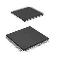
DF2166VT33WV Renesas Electronics America, DF2166VT33WV Datasheet - Page 763

DF2166VT33WV
Manufacturer Part Number
DF2166VT33WV
Description
MCU 16BIT FLASH 3V 512K 144-TQFP
Manufacturer
Renesas Electronics America
Series
H8® H8S/2100r
Datasheet
1.HS2168EPI61H-U.pdf
(876 pages)
Specifications of DF2166VT33WV
Core Processor
H8S/2000
Core Size
16-Bit
Speed
33MHz
Connectivity
I²C, IrDA, LPC, SCI, SmartCard
Peripherals
POR, PWM, WDT
Number Of I /o
106
Program Memory Size
512KB (512K x 8)
Program Memory Type
FLASH
Ram Size
40K x 8
Voltage - Supply (vcc/vdd)
3 V ~ 3.6 V
Data Converters
A/D 8x10b; D/A 2x8b
Oscillator Type
External
Operating Temperature
-20°C ~ 75°C
Package / Case
144-TQFP, 144-VQFP
Lead Free Status / RoHS Status
Lead free / RoHS Compliant
Eeprom Size
-
Available stocks
Company
Part Number
Manufacturer
Quantity
Price
Company:
Part Number:
DF2166VT33WV
Manufacturer:
Renesas Electronics America
Quantity:
135
Company:
Part Number:
DF2166VT33WV
Manufacturer:
Renesas Electronics America
Quantity:
10 000
- Current page: 763 of 876
- Download datasheet (5Mb)
This LSI incorporates a clock pulse generator which generates the system clock (φ), internal clock,
bus master clock, and subclock (φSUB). The clock pulse generator consists of an oscillator, PLL
multiplier circuit, system clock select circuit, medium-speed clock divider, bus master clock select
circuit, subclock input circuit, and subclock waveform forming circuit. Figure 22.1 shows a block
diagram of the clock pulse generator.
The bus master clock is selected as either high-speed mode or medium-speed mode by software
according to the settings of the SCK2 to SCK0 bits in the standby control register. Use of the
medium-speed clock (φ/2 to φ/32) may be limited during CPU operation and when accessing the
internal memory of the CPU. The operation speed of the DTC and the external space access cycle
are thus stabilized regardless of the setting of medium-speed mode. For details on the standby
control register, see section 23.1.1, Standby Control Register (SBYCR).
The subclock input is controlled by software according to the EXCLE bit setting in the low power
control register. For details on the low power control register, see section 23.1.2, Low-Power
Control Register (LPWRCR).
CPG0500A_000120020900
EXTAL
PFSEL
EXCL
XTAL
input circuit
Subclock
Oscillator
Figure 22.1 Block Diagram of Clock Pulse Generator
Section 22 Clock Pulse Generator
waveform
multiplier
Subclock
forming
circuit
circuit
PLL
count clock
φSUB
WDT_1
φ
System clock
select circuit
System clock
to φ pin
φ
Rev. 3.00, 03/04, page 721 of 830
speed clock
Medium-
divider
Internal clock
to peripheral
modules
φ/2
to φ/32
clock select
Bus master
circuit
Bus master clock
to CPU and DTC
Related parts for DF2166VT33WV
Image
Part Number
Description
Manufacturer
Datasheet
Request
R

Part Number:
Description:
KIT STARTER FOR M16C/29
Manufacturer:
Renesas Electronics America
Datasheet:

Part Number:
Description:
KIT STARTER FOR R8C/2D
Manufacturer:
Renesas Electronics America
Datasheet:

Part Number:
Description:
R0K33062P STARTER KIT
Manufacturer:
Renesas Electronics America
Datasheet:

Part Number:
Description:
KIT STARTER FOR R8C/23 E8A
Manufacturer:
Renesas Electronics America
Datasheet:

Part Number:
Description:
KIT STARTER FOR R8C/25
Manufacturer:
Renesas Electronics America
Datasheet:

Part Number:
Description:
KIT STARTER H8S2456 SHARPE DSPLY
Manufacturer:
Renesas Electronics America
Datasheet:

Part Number:
Description:
KIT STARTER FOR R8C38C
Manufacturer:
Renesas Electronics America
Datasheet:

Part Number:
Description:
KIT STARTER FOR R8C35C
Manufacturer:
Renesas Electronics America
Datasheet:

Part Number:
Description:
KIT STARTER FOR R8CL3AC+LCD APPS
Manufacturer:
Renesas Electronics America
Datasheet:

Part Number:
Description:
KIT STARTER FOR RX610
Manufacturer:
Renesas Electronics America
Datasheet:

Part Number:
Description:
KIT STARTER FOR R32C/118
Manufacturer:
Renesas Electronics America
Datasheet:

Part Number:
Description:
KIT DEV RSK-R8C/26-29
Manufacturer:
Renesas Electronics America
Datasheet:

Part Number:
Description:
KIT STARTER FOR SH7124
Manufacturer:
Renesas Electronics America
Datasheet:

Part Number:
Description:
KIT STARTER FOR H8SX/1622
Manufacturer:
Renesas Electronics America
Datasheet:

Part Number:
Description:
KIT DEV FOR SH7203
Manufacturer:
Renesas Electronics America
Datasheet:


