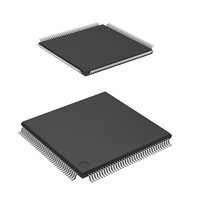
DF2166VT33WV Renesas Electronics America, DF2166VT33WV Datasheet - Page 352

DF2166VT33WV
Manufacturer Part Number
DF2166VT33WV
Description
MCU 16BIT FLASH 3V 512K 144-TQFP
Manufacturer
Renesas Electronics America
Series
H8® H8S/2100r
Datasheet
1.HS2168EPI61H-U.pdf
(876 pages)
Specifications of DF2166VT33WV
Core Processor
H8S/2000
Core Size
16-Bit
Speed
33MHz
Connectivity
I²C, IrDA, LPC, SCI, SmartCard
Peripherals
POR, PWM, WDT
Number Of I /o
106
Program Memory Size
512KB (512K x 8)
Program Memory Type
FLASH
Ram Size
40K x 8
Voltage - Supply (vcc/vdd)
3 V ~ 3.6 V
Data Converters
A/D 8x10b; D/A 2x8b
Oscillator Type
External
Operating Temperature
-20°C ~ 75°C
Package / Case
144-TQFP, 144-VQFP
Lead Free Status / RoHS Status
Lead free / RoHS Compliant
Eeprom Size
-
Available stocks
Company
Part Number
Manufacturer
Quantity
Price
Company:
Part Number:
DF2166VT33WV
Manufacturer:
Renesas Electronics America
Quantity:
135
Company:
Part Number:
DF2166VT33WV
Manufacturer:
Renesas Electronics America
Quantity:
10 000
- Current page: 352 of 876
- Download datasheet (5Mb)
12.3.2
TCORA is an 8-bit readable/writable register. TCORA_0 and TCORA_1 comprise a single 16-bit
register, so they can be accessed together by word access. TCORA is continually compared with
the value in TCNT. When a match is detected, the corresponding compare-match flag A (CMFA)
in TCSR is set to 1. Note however that comparison is disabled during the T2 state of a TCORA
write cycle. The timer output from the TMO pin can be freely controlled by these compare-match
A signals and the settings of output select bits OS1 and OS0 in TCSR. TCORA is initialized to
H'FF.
TCORA_Y can be accessed when the KINWUE bit in SYSCR is 0 and the TMRX/Y bit in
TCONRS is 1. TCORA_X can be accessed when the KINWUE bit in SYSCR is 0 and the
TMRX/Y bit in TCONRS is 0. See section 3.2.2, System Control Register (SYSCR), and section
12.3.11, Timer Connection Register S (TCONRS).
12.3.3
TCORB is an 8-bit readable/writable register. TCORB_0 and TCORB_ comprise a single 16-bit
register, so they can be accessed together by word access. TCORB is continually compared with
the value in TCNT. When a match is detected, the corresponding compare-match flag B (CMFB)
in TCSR is set to 1. Note however that comparison is disabled during the T2 state of a TCORB
write cycle. The timer output from the TMO pin can be freely controlled by these compare-match
B signals and the settings of output select bits OS3 and OS2 in TCSR. TCORB is initialized to
H'FF.
TCORB_Y can be accessed when the KINWUE bit in SYSCR is 0 and the TMRX/Y bit in
TCONRS is 1. TCORB_X can be accessed when the KINWUE bit in SYSCR is 0 and the
TMRX/Y bit in TCONRS is 0. See section 3.2.2, System Control Register (SYSCR), and section
12.3.11, Timer Connection Register S (TCONRS).
Rev. 3.00, 03/04, page 310 of 830
Time Constant Register A (TCORA)
Time Constant Register B (TCORB)
Related parts for DF2166VT33WV
Image
Part Number
Description
Manufacturer
Datasheet
Request
R

Part Number:
Description:
KIT STARTER FOR M16C/29
Manufacturer:
Renesas Electronics America
Datasheet:

Part Number:
Description:
KIT STARTER FOR R8C/2D
Manufacturer:
Renesas Electronics America
Datasheet:

Part Number:
Description:
R0K33062P STARTER KIT
Manufacturer:
Renesas Electronics America
Datasheet:

Part Number:
Description:
KIT STARTER FOR R8C/23 E8A
Manufacturer:
Renesas Electronics America
Datasheet:

Part Number:
Description:
KIT STARTER FOR R8C/25
Manufacturer:
Renesas Electronics America
Datasheet:

Part Number:
Description:
KIT STARTER H8S2456 SHARPE DSPLY
Manufacturer:
Renesas Electronics America
Datasheet:

Part Number:
Description:
KIT STARTER FOR R8C38C
Manufacturer:
Renesas Electronics America
Datasheet:

Part Number:
Description:
KIT STARTER FOR R8C35C
Manufacturer:
Renesas Electronics America
Datasheet:

Part Number:
Description:
KIT STARTER FOR R8CL3AC+LCD APPS
Manufacturer:
Renesas Electronics America
Datasheet:

Part Number:
Description:
KIT STARTER FOR RX610
Manufacturer:
Renesas Electronics America
Datasheet:

Part Number:
Description:
KIT STARTER FOR R32C/118
Manufacturer:
Renesas Electronics America
Datasheet:

Part Number:
Description:
KIT DEV RSK-R8C/26-29
Manufacturer:
Renesas Electronics America
Datasheet:

Part Number:
Description:
KIT STARTER FOR SH7124
Manufacturer:
Renesas Electronics America
Datasheet:

Part Number:
Description:
KIT STARTER FOR H8SX/1622
Manufacturer:
Renesas Electronics America
Datasheet:

Part Number:
Description:
KIT DEV FOR SH7203
Manufacturer:
Renesas Electronics America
Datasheet:


