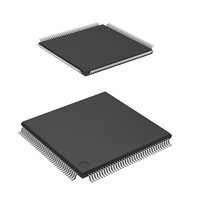
DF2166VT33WV Renesas Electronics America, DF2166VT33WV Datasheet - Page 259

DF2166VT33WV
Manufacturer Part Number
DF2166VT33WV
Description
MCU 16BIT FLASH 3V 512K 144-TQFP
Manufacturer
Renesas Electronics America
Series
H8® H8S/2100r
Datasheet
1.HS2168EPI61H-U.pdf
(876 pages)
Specifications of DF2166VT33WV
Core Processor
H8S/2000
Core Size
16-Bit
Speed
33MHz
Connectivity
I²C, IrDA, LPC, SCI, SmartCard
Peripherals
POR, PWM, WDT
Number Of I /o
106
Program Memory Size
512KB (512K x 8)
Program Memory Type
FLASH
Ram Size
40K x 8
Voltage - Supply (vcc/vdd)
3 V ~ 3.6 V
Data Converters
A/D 8x10b; D/A 2x8b
Oscillator Type
External
Operating Temperature
-20°C ~ 75°C
Package / Case
144-TQFP, 144-VQFP
Lead Free Status / RoHS Status
Lead free / RoHS Compliant
Eeprom Size
-
Available stocks
Company
Part Number
Manufacturer
Quantity
Price
Company:
Part Number:
DF2166VT33WV
Manufacturer:
Renesas Electronics America
Quantity:
135
Company:
Part Number:
DF2166VT33WV
Manufacturer:
Renesas Electronics America
Quantity:
10 000
- Current page: 259 of 876
- Download datasheet (5Mb)
8.8
Port 8 is an 8-bit I/O port. Port 8 pins also function as the A/D converter external trigger input pin,
SCI_0, SCI_1, and SCI_2 clock input/output pins, IIC_0 and IIC_1 input/output pins, TMR_0,
TMR_1, TMR_X, and TMR_Y input pins, and interrupt input pins. Port 8 is an NMOS push-pull
output. Port 8 has the following registers.
• Port 8 data direction register (P8DDR)
• Port 8 data register (P8DR)
8.8.1
The individual bits of P8DDR specify input or output for the pins of port 8.
8.8.2
P8DR stores output data for the port 8 pins.
Bit
7
6
5
4
3
2
1
0
Bit
7
6
5
4
3
2
1
0
Bit Name
P87DDR
P86DDR
P85DDR
P84DDR
P83DDR
P82DDR
P81DDR
P80DDR
Bit Name
P87DR
P86DR
P85DR
P84DR
P83DR
P82DR
P81DR
P80DR
Port 8
Port 8 Data Direction Register (P8DDR)
Port 8 Data Register (P8DR)
Initial Value
0
0
0
0
0
0
0
0
Initial Value
0
0
0
0
0
0
0
0
R/W
W
W
W
W
W
W
W
W
R/W
R/W
R/W
R/W
R/W
R/W
R/W
R/W
R/W
Description
This register is assigned to the same address as that
of PBPIN. When this register is read, the port B states
are read.
If port 8 pins are specified for use as the general I/O
port, the corresponding port 8 pins are output ports
when the P8DDR bits are set to 1, and input ports
when cleared to 0.
Description
P8DR stores output data for the port 8 pins that are
used as the general output port.
If a port 8 read is performed while the P8DDR bits are
set to 1, the P8DR values are read. If a port 8 read is
performed while the P8DDR bits are cleared to 0, the
pin states are read.
Rev. 3.00, 03/04, page 217 of 830
Related parts for DF2166VT33WV
Image
Part Number
Description
Manufacturer
Datasheet
Request
R

Part Number:
Description:
KIT STARTER FOR M16C/29
Manufacturer:
Renesas Electronics America
Datasheet:

Part Number:
Description:
KIT STARTER FOR R8C/2D
Manufacturer:
Renesas Electronics America
Datasheet:

Part Number:
Description:
R0K33062P STARTER KIT
Manufacturer:
Renesas Electronics America
Datasheet:

Part Number:
Description:
KIT STARTER FOR R8C/23 E8A
Manufacturer:
Renesas Electronics America
Datasheet:

Part Number:
Description:
KIT STARTER FOR R8C/25
Manufacturer:
Renesas Electronics America
Datasheet:

Part Number:
Description:
KIT STARTER H8S2456 SHARPE DSPLY
Manufacturer:
Renesas Electronics America
Datasheet:

Part Number:
Description:
KIT STARTER FOR R8C38C
Manufacturer:
Renesas Electronics America
Datasheet:

Part Number:
Description:
KIT STARTER FOR R8C35C
Manufacturer:
Renesas Electronics America
Datasheet:

Part Number:
Description:
KIT STARTER FOR R8CL3AC+LCD APPS
Manufacturer:
Renesas Electronics America
Datasheet:

Part Number:
Description:
KIT STARTER FOR RX610
Manufacturer:
Renesas Electronics America
Datasheet:

Part Number:
Description:
KIT STARTER FOR R32C/118
Manufacturer:
Renesas Electronics America
Datasheet:

Part Number:
Description:
KIT DEV RSK-R8C/26-29
Manufacturer:
Renesas Electronics America
Datasheet:

Part Number:
Description:
KIT STARTER FOR SH7124
Manufacturer:
Renesas Electronics America
Datasheet:

Part Number:
Description:
KIT STARTER FOR H8SX/1622
Manufacturer:
Renesas Electronics America
Datasheet:

Part Number:
Description:
KIT DEV FOR SH7203
Manufacturer:
Renesas Electronics America
Datasheet:


