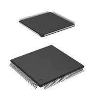
DF2166VT33WV Renesas Electronics America, DF2166VT33WV Datasheet - Page 160

DF2166VT33WV
Manufacturer Part Number
DF2166VT33WV
Description
MCU 16BIT FLASH 3V 512K 144-TQFP
Manufacturer
Renesas Electronics America
Series
H8® H8S/2100r
Datasheet
1.HS2168EPI61H-U.pdf
(876 pages)
Specifications of DF2166VT33WV
Core Processor
H8S/2000
Core Size
16-Bit
Speed
33MHz
Connectivity
I²C, IrDA, LPC, SCI, SmartCard
Peripherals
POR, PWM, WDT
Number Of I /o
106
Program Memory Size
512KB (512K x 8)
Program Memory Type
FLASH
Ram Size
40K x 8
Voltage - Supply (vcc/vdd)
3 V ~ 3.6 V
Data Converters
A/D 8x10b; D/A 2x8b
Oscillator Type
External
Operating Temperature
-20°C ~ 75°C
Package / Case
144-TQFP, 144-VQFP
Lead Free Status / RoHS Status
Lead free / RoHS Compliant
Eeprom Size
-
Available stocks
Company
Part Number
Manufacturer
Quantity
Price
Company:
Part Number:
DF2166VT33WV
Manufacturer:
Renesas Electronics America
Quantity:
135
Company:
Part Number:
DF2166VT33WV
Manufacturer:
Renesas Electronics America
Quantity:
10 000
- Current page: 160 of 876
- Download datasheet (5Mb)
(2) In Address-Data Multiplex Extended Mode
(a) Bus Width: A bus width of 8 or 16 bits can be selected via the ABW and ABW256 bits in
WSCR, and the ABWCP bit in BCR2.
(b) Number of Access States: Two or three states can be selected for data access via the AST and
AST256 bits in WSCR, and the ASTCP bit in BCR2. When the 2-state access space is designated,
wait-state insertion is disabled.
(c) Wait Mode and Number of Program Wait States:
i)
When the IOS extended area is specified as a 3-state access space by the AST bit in WSCR, the
wait mode and the number of program wait states to be inserted automatically is selected by the
WMS1, WMS0, WC1, and WC0 bits in WSCR. Zero or one program wait state can be inserted
into address cycle. From zero to three program wait states can be selected for data cycle.
ii)
When the 256-kbyte extended area is specified as a 3-state access space by the AST256 bit in
WSCR, the wait mode and the number of program wait states to be inserted automatically is
selected by the WMS10, WC11, and WC10 bits in WSCR2. Zero or one program wait state can be
inserted into address cycle. From zero to three program wait states can be selected for data cycle.
iii)
When the CP extended area is specified as a 3-state access space by the ASTCP bit in BCR2, the
wait mode and the number of program wait states to be inserted automatically is selected by the
WMS21, WMS20, WC22, WC21, and WC20 bits in WSCR2. Zero or one program wait state can
be inserted into address cycle. From zero to three program wait states can be selected for data
cycle.
The wait function for external extension is effective for connecting low-speed devices to the
external address space. However, this wait function may cause some problems when the operation
of bus masters other than the CPU, such as the DTC, are to be delayed.
Tables 6.7 to 6.14 show address-data multiplex address space and the bus specifications for the
basic bus interface of each area.
Rev. 3.00, 03/04, page 118 of 830
IOS Extended Area
256-kbyte Extended Area
CP Extended Area
Related parts for DF2166VT33WV
Image
Part Number
Description
Manufacturer
Datasheet
Request
R

Part Number:
Description:
KIT STARTER FOR M16C/29
Manufacturer:
Renesas Electronics America
Datasheet:

Part Number:
Description:
KIT STARTER FOR R8C/2D
Manufacturer:
Renesas Electronics America
Datasheet:

Part Number:
Description:
R0K33062P STARTER KIT
Manufacturer:
Renesas Electronics America
Datasheet:

Part Number:
Description:
KIT STARTER FOR R8C/23 E8A
Manufacturer:
Renesas Electronics America
Datasheet:

Part Number:
Description:
KIT STARTER FOR R8C/25
Manufacturer:
Renesas Electronics America
Datasheet:

Part Number:
Description:
KIT STARTER H8S2456 SHARPE DSPLY
Manufacturer:
Renesas Electronics America
Datasheet:

Part Number:
Description:
KIT STARTER FOR R8C38C
Manufacturer:
Renesas Electronics America
Datasheet:

Part Number:
Description:
KIT STARTER FOR R8C35C
Manufacturer:
Renesas Electronics America
Datasheet:

Part Number:
Description:
KIT STARTER FOR R8CL3AC+LCD APPS
Manufacturer:
Renesas Electronics America
Datasheet:

Part Number:
Description:
KIT STARTER FOR RX610
Manufacturer:
Renesas Electronics America
Datasheet:

Part Number:
Description:
KIT STARTER FOR R32C/118
Manufacturer:
Renesas Electronics America
Datasheet:

Part Number:
Description:
KIT DEV RSK-R8C/26-29
Manufacturer:
Renesas Electronics America
Datasheet:

Part Number:
Description:
KIT STARTER FOR SH7124
Manufacturer:
Renesas Electronics America
Datasheet:

Part Number:
Description:
KIT STARTER FOR H8SX/1622
Manufacturer:
Renesas Electronics America
Datasheet:

Part Number:
Description:
KIT DEV FOR SH7203
Manufacturer:
Renesas Electronics America
Datasheet:


