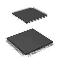
DF2166VT33WV Renesas Electronics America, DF2166VT33WV Datasheet - Page 710

DF2166VT33WV
Manufacturer Part Number
DF2166VT33WV
Description
MCU 16BIT FLASH 3V 512K 144-TQFP
Manufacturer
Renesas Electronics America
Series
H8® H8S/2100r
Datasheet
1.HS2168EPI61H-U.pdf
(876 pages)
Specifications of DF2166VT33WV
Core Processor
H8S/2000
Core Size
16-Bit
Speed
33MHz
Connectivity
I²C, IrDA, LPC, SCI, SmartCard
Peripherals
POR, PWM, WDT
Number Of I /o
106
Program Memory Size
512KB (512K x 8)
Program Memory Type
FLASH
Ram Size
40K x 8
Voltage - Supply (vcc/vdd)
3 V ~ 3.6 V
Data Converters
A/D 8x10b; D/A 2x8b
Oscillator Type
External
Operating Temperature
-20°C ~ 75°C
Package / Case
144-TQFP, 144-VQFP
Lead Free Status / RoHS Status
Lead free / RoHS Compliant
Eeprom Size
-
Available stocks
Company
Part Number
Manufacturer
Quantity
Price
Company:
Part Number:
DF2166VT33WV
Manufacturer:
Renesas Electronics America
Quantity:
135
Company:
Part Number:
DF2166VT33WV
Manufacturer:
Renesas Electronics America
Quantity:
10 000
- Current page: 710 of 876
- Download datasheet (5Mb)
20.6
It is possible to alternate between the user MAT and user boot MAT. However, the following
procedure is required because these MATs are allocated to address 0.
(Switching to the user boot MAT disables programming and erasing. Programming of the user
boot MAT should take place in boot mode or programmer mode.)
1. MAT switching by FMATS should always be executed from the on-chip RAM.
2. To ensure that the MAT that has been switched to is accessible, execute four NOP instructions
3. If an interrupt has occurred during switching, there is no guarantee of which memory MAT is
4. After the MATs have been switched, take care because the interrupt vector table will also have
5. Memory sizes of the user MAT and user boot MAT are different. When accessing the user
Rev. 3.00, 03/04, page 668 of 830
in the on-chip RAM immediately after writing to FMATS of the on-chip RAM (this prevents
access to the flash memory during MAT switching).
being accessed. Always mask the maskable interrupts before switching between MATs. In
addition, configure the system so that NMI interrupts do not occur during MAT switching.
been switched. If interrupt processing is to be the same before and after MAT switching,
transfer the interrupt-processing routines to the on-chip RAM and set the WEINTE bit in
FCCS to place the interrupt-vector table in the on-chip RAM.
boot MAT, do not access addresses above the top of its 8-kbyte memory space. If access goes
beyond the 8-kbyte space, the values read are undefined.
Switching between User MAT and User Boot MAT
Figure 20.17 Switching between the User MAT and User Boot MAT
< User MAT >
Procedure for switching to the user boot MAT
(1) Mask interrupts
(2) Write H'AA to FMATS.
(3) Execute four NOP instructions before
Procedure for switching to the user MAT
(1) Mask interrupts
(2) Write a value other than H'AA to FMATS.
(3) Execute four NOP instructions before accessing
accessing the user boot MAT.
the user MAT.
< On-chip RAM >
switching to the
user boot MAT
Procedure for
Procedure for
the user MAT
switching to
< User boot MAT >
Related parts for DF2166VT33WV
Image
Part Number
Description
Manufacturer
Datasheet
Request
R

Part Number:
Description:
KIT STARTER FOR M16C/29
Manufacturer:
Renesas Electronics America
Datasheet:

Part Number:
Description:
KIT STARTER FOR R8C/2D
Manufacturer:
Renesas Electronics America
Datasheet:

Part Number:
Description:
R0K33062P STARTER KIT
Manufacturer:
Renesas Electronics America
Datasheet:

Part Number:
Description:
KIT STARTER FOR R8C/23 E8A
Manufacturer:
Renesas Electronics America
Datasheet:

Part Number:
Description:
KIT STARTER FOR R8C/25
Manufacturer:
Renesas Electronics America
Datasheet:

Part Number:
Description:
KIT STARTER H8S2456 SHARPE DSPLY
Manufacturer:
Renesas Electronics America
Datasheet:

Part Number:
Description:
KIT STARTER FOR R8C38C
Manufacturer:
Renesas Electronics America
Datasheet:

Part Number:
Description:
KIT STARTER FOR R8C35C
Manufacturer:
Renesas Electronics America
Datasheet:

Part Number:
Description:
KIT STARTER FOR R8CL3AC+LCD APPS
Manufacturer:
Renesas Electronics America
Datasheet:

Part Number:
Description:
KIT STARTER FOR RX610
Manufacturer:
Renesas Electronics America
Datasheet:

Part Number:
Description:
KIT STARTER FOR R32C/118
Manufacturer:
Renesas Electronics America
Datasheet:

Part Number:
Description:
KIT DEV RSK-R8C/26-29
Manufacturer:
Renesas Electronics America
Datasheet:

Part Number:
Description:
KIT STARTER FOR SH7124
Manufacturer:
Renesas Electronics America
Datasheet:

Part Number:
Description:
KIT STARTER FOR H8SX/1622
Manufacturer:
Renesas Electronics America
Datasheet:

Part Number:
Description:
KIT DEV FOR SH7203
Manufacturer:
Renesas Electronics America
Datasheet:


