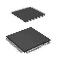
DF2166VT33WV Renesas Electronics America, DF2166VT33WV Datasheet - Page 549

DF2166VT33WV
Manufacturer Part Number
DF2166VT33WV
Description
MCU 16BIT FLASH 3V 512K 144-TQFP
Manufacturer
Renesas Electronics America
Series
H8® H8S/2100r
Datasheet
1.HS2168EPI61H-U.pdf
(876 pages)
Specifications of DF2166VT33WV
Core Processor
H8S/2000
Core Size
16-Bit
Speed
33MHz
Connectivity
I²C, IrDA, LPC, SCI, SmartCard
Peripherals
POR, PWM, WDT
Number Of I /o
106
Program Memory Size
512KB (512K x 8)
Program Memory Type
FLASH
Ram Size
40K x 8
Voltage - Supply (vcc/vdd)
3 V ~ 3.6 V
Data Converters
A/D 8x10b; D/A 2x8b
Oscillator Type
External
Operating Temperature
-20°C ~ 75°C
Package / Case
144-TQFP, 144-VQFP
Lead Free Status / RoHS Status
Lead free / RoHS Compliant
Eeprom Size
-
Available stocks
Company
Part Number
Manufacturer
Quantity
Price
Company:
Part Number:
DF2166VT33WV
Manufacturer:
Renesas Electronics America
Quantity:
135
Company:
Part Number:
DF2166VT33WV
Manufacturer:
Renesas Electronics America
Quantity:
10 000
- Current page: 549 of 876
- Download datasheet (5Mb)
This LSI has an on-chip LPC interface.
The LPC performs serial transfer of cycle type, address, and data, synchronized with the 33 MHz
PCI clock. It uses four signal lines for address/data, and one for host interrupt requests. The LPC
interface operates as a slave and supports only I/O read cycle and I/O write cycle transfer.
It is also provided with power-down functions that can control the PCI clock and shut down the
LPC interface.
16.1
• Supports LPC interface I/O read cycles and I/O write cycles
• Has three register sets comprising data and status registers
• Supports SERIRQ
• Power-down functions, interrupts, etc.
• Supports version 1.5 of the Intelligent Platform Management Interface (IPMI)
IFHSTL1A_010020030700
Uses four signal lines (LAD3 to LAD0) to transfer the cycle type, address, and data.
Uses three control signals: clock (LCLK), reset (LRESET), and frame (LFRAME).
The basic register set comprises three bytes: an input register (IDR), output register (ODR),
and status register (STR).
Channels 1 to 3 have fixed I/O addresses of H'0000 to H'FFFF, respectively.
A fast A20 gate function is also provided.
Sixteen bidirectional data register bytes can be manipulated in addition to the basic register set.
Host interrupt requests are transferred serially on a single signal line (SERIRQ).
On channel 1, HIRQ1 and HIRQ12 can be generated.
On channels 2 and 3, SMI, HIRQ6, and HIRQ9 to HIRQ11 can be generated.
Operation can be switched between quiet mode and continuous mode.
The CLKRUN signal can be manipulated to restart the PCI clock (LCLK).
The LPC module can be shut down by inputting the LPCPD signal.
Three pins, PME, LSMI, and LSCI, are provided for general input/output.
Channel 3 supports the SMIC interface, KCS interface, and BT interface.
Features
Section 16 LPC Interface (LPC)
Rev. 3.00, 03/04, page 507 of 830
Related parts for DF2166VT33WV
Image
Part Number
Description
Manufacturer
Datasheet
Request
R

Part Number:
Description:
KIT STARTER FOR M16C/29
Manufacturer:
Renesas Electronics America
Datasheet:

Part Number:
Description:
KIT STARTER FOR R8C/2D
Manufacturer:
Renesas Electronics America
Datasheet:

Part Number:
Description:
R0K33062P STARTER KIT
Manufacturer:
Renesas Electronics America
Datasheet:

Part Number:
Description:
KIT STARTER FOR R8C/23 E8A
Manufacturer:
Renesas Electronics America
Datasheet:

Part Number:
Description:
KIT STARTER FOR R8C/25
Manufacturer:
Renesas Electronics America
Datasheet:

Part Number:
Description:
KIT STARTER H8S2456 SHARPE DSPLY
Manufacturer:
Renesas Electronics America
Datasheet:

Part Number:
Description:
KIT STARTER FOR R8C38C
Manufacturer:
Renesas Electronics America
Datasheet:

Part Number:
Description:
KIT STARTER FOR R8C35C
Manufacturer:
Renesas Electronics America
Datasheet:

Part Number:
Description:
KIT STARTER FOR R8CL3AC+LCD APPS
Manufacturer:
Renesas Electronics America
Datasheet:

Part Number:
Description:
KIT STARTER FOR RX610
Manufacturer:
Renesas Electronics America
Datasheet:

Part Number:
Description:
KIT STARTER FOR R32C/118
Manufacturer:
Renesas Electronics America
Datasheet:

Part Number:
Description:
KIT DEV RSK-R8C/26-29
Manufacturer:
Renesas Electronics America
Datasheet:

Part Number:
Description:
KIT STARTER FOR SH7124
Manufacturer:
Renesas Electronics America
Datasheet:

Part Number:
Description:
KIT STARTER FOR H8SX/1622
Manufacturer:
Renesas Electronics America
Datasheet:

Part Number:
Description:
KIT DEV FOR SH7203
Manufacturer:
Renesas Electronics America
Datasheet:


