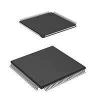
DF2166VT33WV Renesas Electronics America, DF2166VT33WV Datasheet - Page 569

DF2166VT33WV
Manufacturer Part Number
DF2166VT33WV
Description
MCU 16BIT FLASH 3V 512K 144-TQFP
Manufacturer
Renesas Electronics America
Series
H8® H8S/2100r
Datasheet
1.HS2168EPI61H-U.pdf
(876 pages)
Specifications of DF2166VT33WV
Core Processor
H8S/2000
Core Size
16-Bit
Speed
33MHz
Connectivity
I²C, IrDA, LPC, SCI, SmartCard
Peripherals
POR, PWM, WDT
Number Of I /o
106
Program Memory Size
512KB (512K x 8)
Program Memory Type
FLASH
Ram Size
40K x 8
Voltage - Supply (vcc/vdd)
3 V ~ 3.6 V
Data Converters
A/D 8x10b; D/A 2x8b
Oscillator Type
External
Operating Temperature
-20°C ~ 75°C
Package / Case
144-TQFP, 144-VQFP
Lead Free Status / RoHS Status
Lead free / RoHS Compliant
Eeprom Size
-
Available stocks
Company
Part Number
Manufacturer
Quantity
Price
Company:
Part Number:
DF2166VT33WV
Manufacturer:
Renesas Electronics America
Quantity:
135
Company:
Part Number:
DF2166VT33WV
Manufacturer:
Renesas Electronics America
Quantity:
10 000
- Current page: 569 of 876
- Download datasheet (5Mb)
Table 16.4 Slave Selection Internal Registers
16.3.6
The IDR registers are 8-bit read-only registers to the slave processor (this LSI), and 8-bit write-
only registers to the host processor. The registers selected from the host according to the I/O
address are described in the following sections: for information on IDR1 and IDR2 selection, see
section 16.3.5, LPC Channel 1, 2 Address Register H, L (LADR12H, LADR12L), and for
information on IDR3 selection, see section 16.3.4, LPC Channel 3 Address Register H, L
(LADR3H, LADR3L). Data transferred in an LPC I/O write cycle is written to the selected
register. The state of bit 2 of the I/O address is latched into the C/D bit in STR, to indicate whether
the written information is a command or data.
The initial values of the IDR registers are undefined.
16.3.7
The ODR registers are 8-bit readable/writable registers to the slave processor (this LSI), and 8-bit
read-only registers to the host processor. The registers selected from the host according to the I/O
address are described in the following sections: for information on ODR1 and ODR2 selection, see
section 16.3.5, LPC Channel 1, 2 Address Register H, L (LADR12H, LADR12L), and for
information on ODR3 selection, see section 16.3.4, LPC Channel 3 Address Register H, L
(LADR3H, LADR3L). In an LPC I/O read cycle, the data in the selected register is transferred to
the host.
The initial values of the ODR registers are undefined.
Slave (R/W) Bus Width (B/W) LADR12SEL
R/W
R/W
R/W
R/W
R/W
R/W
Input Data Registers 1 to 3 (IDR1 to IDR3)
Output Data Registers 0 to 3 (ODR1 to ODR3)
B
B
B
B
W
W
0
1
0
1
0
1
LADR12H
LADR12H
LADR12H LADR12L
LADR12H LADR12L
LADR12
LADR12L
LADR12L
Rev. 3.00, 03/04, page 527 of 830
LADR1H
LADR2H
LADR1H
LADR2H
Internal Register
LADR1L
LADR2L
LADR1L
LADR2L
Related parts for DF2166VT33WV
Image
Part Number
Description
Manufacturer
Datasheet
Request
R

Part Number:
Description:
KIT STARTER FOR M16C/29
Manufacturer:
Renesas Electronics America
Datasheet:

Part Number:
Description:
KIT STARTER FOR R8C/2D
Manufacturer:
Renesas Electronics America
Datasheet:

Part Number:
Description:
R0K33062P STARTER KIT
Manufacturer:
Renesas Electronics America
Datasheet:

Part Number:
Description:
KIT STARTER FOR R8C/23 E8A
Manufacturer:
Renesas Electronics America
Datasheet:

Part Number:
Description:
KIT STARTER FOR R8C/25
Manufacturer:
Renesas Electronics America
Datasheet:

Part Number:
Description:
KIT STARTER H8S2456 SHARPE DSPLY
Manufacturer:
Renesas Electronics America
Datasheet:

Part Number:
Description:
KIT STARTER FOR R8C38C
Manufacturer:
Renesas Electronics America
Datasheet:

Part Number:
Description:
KIT STARTER FOR R8C35C
Manufacturer:
Renesas Electronics America
Datasheet:

Part Number:
Description:
KIT STARTER FOR R8CL3AC+LCD APPS
Manufacturer:
Renesas Electronics America
Datasheet:

Part Number:
Description:
KIT STARTER FOR RX610
Manufacturer:
Renesas Electronics America
Datasheet:

Part Number:
Description:
KIT STARTER FOR R32C/118
Manufacturer:
Renesas Electronics America
Datasheet:

Part Number:
Description:
KIT DEV RSK-R8C/26-29
Manufacturer:
Renesas Electronics America
Datasheet:

Part Number:
Description:
KIT STARTER FOR SH7124
Manufacturer:
Renesas Electronics America
Datasheet:

Part Number:
Description:
KIT STARTER FOR H8SX/1622
Manufacturer:
Renesas Electronics America
Datasheet:

Part Number:
Description:
KIT DEV FOR SH7203
Manufacturer:
Renesas Electronics America
Datasheet:


