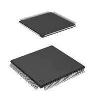
DF2166VT33WV Renesas Electronics America, DF2166VT33WV Datasheet - Page 361

DF2166VT33WV
Manufacturer Part Number
DF2166VT33WV
Description
MCU 16BIT FLASH 3V 512K 144-TQFP
Manufacturer
Renesas Electronics America
Series
H8® H8S/2100r
Datasheet
1.HS2168EPI61H-U.pdf
(876 pages)
Specifications of DF2166VT33WV
Core Processor
H8S/2000
Core Size
16-Bit
Speed
33MHz
Connectivity
I²C, IrDA, LPC, SCI, SmartCard
Peripherals
POR, PWM, WDT
Number Of I /o
106
Program Memory Size
512KB (512K x 8)
Program Memory Type
FLASH
Ram Size
40K x 8
Voltage - Supply (vcc/vdd)
3 V ~ 3.6 V
Data Converters
A/D 8x10b; D/A 2x8b
Oscillator Type
External
Operating Temperature
-20°C ~ 75°C
Package / Case
144-TQFP, 144-VQFP
Lead Free Status / RoHS Status
Lead free / RoHS Compliant
Eeprom Size
-
Available stocks
Company
Part Number
Manufacturer
Quantity
Price
Company:
Part Number:
DF2166VT33WV
Manufacturer:
Renesas Electronics America
Quantity:
135
Company:
Part Number:
DF2166VT33WV
Manufacturer:
Renesas Electronics America
Quantity:
10 000
- Current page: 361 of 876
- Download datasheet (5Mb)
Note:
12.3.6
TICR is an 8-bit register. The contents of TCNT are transferred to TICR at the rising edge of the
external reset input. TICR cannot be directly accessed by the CPU.
12.3.7
TCORC is an 8-bit readable/writable register. The sum of contents of TCORC and TICR is always
compared with TCNT. When a match is detected, a compare-match C signal is generated.
However, comparison at the T2 state in the write cycle to TCORC and at the input capture cycle of
TICR is disabled. TCORC is initialized to H'FF.
12.3.8
TICRR and TICRF are 8-bit read-only registers. While the ICST bit in TCONRI is set to 1, the
contents of TCNT are transferred at the rising edge and falling edge of the external reset input in
that order. The ICST bit is cleared to 0 when one capture operation ends. TICRR and TICRF are
initialized to H'00.
TICRR and TICRF can be accessed when the KINWUE bit in SYSCR is 0 and the TMRX/Y bit in
TCONRS is 0. See section 3.2.2, System Control Register (SYSCR).
Bit
1
0
*
Input Capture Register (TICR)
Time Constant Register C (TCORC)
Input Capture Registers R and F (TICRR and TICRF)
Only 0 can be written, for flag clearing.
Bit Name Initial Value R/W
OS1
OS0
0
0
R/W
R/W
Description
Output Select 1 and 0
These bits specify how the TMOX pin output level is
to be changed by compare-match A of TCORA_X
and TCNT_X.
00: No change
01: 0 is output
10: 1 is output
11: Output is inverted (toggle output)
Rev. 3.00, 03/04, page 319 of 830
Related parts for DF2166VT33WV
Image
Part Number
Description
Manufacturer
Datasheet
Request
R

Part Number:
Description:
KIT STARTER FOR M16C/29
Manufacturer:
Renesas Electronics America
Datasheet:

Part Number:
Description:
KIT STARTER FOR R8C/2D
Manufacturer:
Renesas Electronics America
Datasheet:

Part Number:
Description:
R0K33062P STARTER KIT
Manufacturer:
Renesas Electronics America
Datasheet:

Part Number:
Description:
KIT STARTER FOR R8C/23 E8A
Manufacturer:
Renesas Electronics America
Datasheet:

Part Number:
Description:
KIT STARTER FOR R8C/25
Manufacturer:
Renesas Electronics America
Datasheet:

Part Number:
Description:
KIT STARTER H8S2456 SHARPE DSPLY
Manufacturer:
Renesas Electronics America
Datasheet:

Part Number:
Description:
KIT STARTER FOR R8C38C
Manufacturer:
Renesas Electronics America
Datasheet:

Part Number:
Description:
KIT STARTER FOR R8C35C
Manufacturer:
Renesas Electronics America
Datasheet:

Part Number:
Description:
KIT STARTER FOR R8CL3AC+LCD APPS
Manufacturer:
Renesas Electronics America
Datasheet:

Part Number:
Description:
KIT STARTER FOR RX610
Manufacturer:
Renesas Electronics America
Datasheet:

Part Number:
Description:
KIT STARTER FOR R32C/118
Manufacturer:
Renesas Electronics America
Datasheet:

Part Number:
Description:
KIT DEV RSK-R8C/26-29
Manufacturer:
Renesas Electronics America
Datasheet:

Part Number:
Description:
KIT STARTER FOR SH7124
Manufacturer:
Renesas Electronics America
Datasheet:

Part Number:
Description:
KIT STARTER FOR H8SX/1622
Manufacturer:
Renesas Electronics America
Datasheet:

Part Number:
Description:
KIT DEV FOR SH7203
Manufacturer:
Renesas Electronics America
Datasheet:


