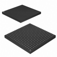
AT91SAM9263B-CU Atmel, AT91SAM9263B-CU Datasheet - Page 908

AT91SAM9263B-CU
Manufacturer Part Number
AT91SAM9263B-CU
Description
IC ARM9 MCU 200 MHZ 324-TFBGA
Manufacturer
Atmel
Series
AT91SAMr
Specifications of AT91SAM9263B-CU
Core Processor
ARM9
Core Size
16/32-Bit
Speed
240MHz
Connectivity
CAN, Ethernet, I²C, MMC, SPI, SSC, UART/USART, USB
Peripherals
AC'97, LCD, POR, PWM, WDT
Number Of I /o
160
Program Memory Size
128KB (128K x 8)
Program Memory Type
ROM
Ram Size
128K x 8
Voltage - Supply (vcc/vdd)
1.08 V ~ 1.32 V
Oscillator Type
Internal
Operating Temperature
-40°C ~ 85°C
Package / Case
324-TFBGA
Processor Series
AT91SAMx
Core
ARM926EJ-S
Data Bus Width
32 bit
Data Ram Size
96 KB
Interface Type
2-Wire, EBI, I2S, MCI, SPI, USART
Maximum Clock Frequency
200 MHz
Number Of Programmable I/os
160
Number Of Timers
4
Maximum Operating Temperature
+ 85 C
Mounting Style
SMD/SMT
3rd Party Development Tools
JTRACE-ARM-2M, MDK-ARM, RL-ARM, ULINK2
Development Tools By Supplier
AT91SAM-ICE, AT91-ISP, AT91SAM9263-EK
Minimum Operating Temperature
- 40 C
Package
324TFBGA
Device Core
ARM926EJ-S
Family Name
91S
Maximum Speed
200 MHz
Operating Supply Voltage
1.8|2.5|3.3 V
Controller Family/series
AT91SAM9xxx
No. Of I/o's
160
Ram Memory Size
96KB
Cpu Speed
240MHz
No. Of Timers
1
Rohs Compliant
Yes
For Use With
AT91SAM9263-EK - KIT EVAL FOR AT91SAM9263AT91SAM-ICE - EMULATOR FOR AT91 ARM7/ARM9
Lead Free Status / RoHS Status
Lead free / RoHS Compliant
Eeprom Size
-
Data Converters
-
Lead Free Status / Rohs Status
Lead free / RoHS Compliant
Other names
Q3735625
Available stocks
Company
Part Number
Manufacturer
Quantity
Price
Company:
Part Number:
AT91SAM9263B-CU
Manufacturer:
IDT
Quantity:
1 043
Part Number:
AT91SAM9263B-CU
Manufacturer:
ATMEL/爱特梅尔
Quantity:
20 000
Company:
Part Number:
AT91SAM9263B-CU-100
Manufacturer:
ATMEL
Quantity:
1 000
- Current page: 908 of 1110
- Download datasheet (17Mb)
Table 44-11. Dithering Algorithm for Color Mode (Continued)
Note:
44.5.2.7
44.5.2.8
908
Frame
N+2
N+2
N+2
N+2
N+2
N+2
…
Ri = red pixel component ON. Gi = green pixel component ON. Bi = blue pixel component ON. ri = red pixel component OFF.
gi = green pixel component OFF. bi = blue pixel component OFF.
AT91SAM9263
green_data_0
green_data_1
blue_data_0
blue_data_1
Shifter
Timegen
red_data_0
red_data_1
Signal
…
The FIFO, Serializer, Palette and Dithering modules process one pixel at a time in monochrome
mode and three sub-pixels at a time in color mode (R,G,B components). This module packs the
data according to the output interface. This interface can be programmed in the DISTYPE,
SCANMOD, and IFWIDTH fields of the LCDCON2 register.
The DISTYPE field selects between TFT, STN monochrome and STN color display. The SCAN-
MODE field selects between single and dual scan modes; in TFT mode, only single scan is
supported. The IFWIDTH field configures the width of the interface in STN mode: 4-bit (in single
scan mode only), 8-bit and 16-bit (in dual scan mode only).
For a more detailed description of the fields, see
page
For a more detailed description of the LCD Interface, see
The time generator block generates the control signals LCDDOTCK, LCDHSYNC, LCDVSYNC,
LCDDEN, used by the LCD module. This block is programmable in order to support different
types of LCD modules and obtain the output clock signals, which are derived from the LCDC
Core clock.
The LCDDOTCK signal is used to clock the data into the LCD drivers' shift register. The data is
sent through LCDD[23:0] synchronized by default with LCDDOTCK falling edge (rising edge can
be selected). The CLKVAL field of LCDCON1 register controls the rate of this signal. The divisor
can also be bypassed with the BYPASS bit in the LCDCON1 register. In this case, the rate of
LCDDOTCK is equal to the frequency of the LCDC Core clock. The minimum period of the LCD-
DOTCK signal depends on the configuration. This information can be found in
The LCDDOTCK signal has two different timings that are selected with the CLKMOD field of the
LCDCON2 register:
• Always Active (used with TFT LCD Modules)
Shadow Level
925.
1010
1010
1010
1010
1010
1010
…
f
LCDDOTCK
Bit used
…
3
2
1
0
3
2
=
-------------------------------- -
2
f
LCDC_clock
×
CLKVAL
Dithering Pattern
0110
0110
0110
0110
0110
0110
…
“LCD Controller (LCDC) User Interface” on
4-bit LCDD
“LCD Interface” on page
LCDD[3]
LCDD[2]
LCDD[1]
LCDD[0]
LCDD[3]
LCDD[2]
…
8-bit LCDD
LCDD[7]
LCDD[6]
LCDD[4]
LCDD[3]
LCDD[5]
LCDD[2]
…
6249H–ATARM–27-Jul-09
Table
913.
44-12.
Output
G0
B0
B1
g1
…
r0
r1
Related parts for AT91SAM9263B-CU
Image
Part Number
Description
Manufacturer
Datasheet
Request
R

Part Number:
Description:
MCU, MPU & DSP Development Tools KICKSTART KIT FOR AT91SAM9 PLUS
Manufacturer:
IAR Systems

Part Number:
Description:
DEV KIT FOR AVR/AVR32
Manufacturer:
Atmel
Datasheet:

Part Number:
Description:
INTERVAL AND WIPE/WASH WIPER CONTROL IC WITH DELAY
Manufacturer:
ATMEL Corporation
Datasheet:

Part Number:
Description:
Low-Voltage Voice-Switched IC for Hands-Free Operation
Manufacturer:
ATMEL Corporation
Datasheet:

Part Number:
Description:
MONOLITHIC INTEGRATED FEATUREPHONE CIRCUIT
Manufacturer:
ATMEL Corporation
Datasheet:

Part Number:
Description:
AM-FM Receiver IC U4255BM-M
Manufacturer:
ATMEL Corporation
Datasheet:

Part Number:
Description:
Monolithic Integrated Feature Phone Circuit
Manufacturer:
ATMEL Corporation
Datasheet:

Part Number:
Description:
Multistandard Video-IF and Quasi Parallel Sound Processing
Manufacturer:
ATMEL Corporation
Datasheet:

Part Number:
Description:
High-performance EE PLD
Manufacturer:
ATMEL Corporation
Datasheet:

Part Number:
Description:
8-bit Flash Microcontroller
Manufacturer:
ATMEL Corporation
Datasheet:

Part Number:
Description:
2-Wire Serial EEPROM
Manufacturer:
ATMEL Corporation
Datasheet:


