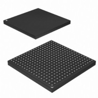
AT91SAM9263B-CU Atmel, AT91SAM9263B-CU Datasheet - Page 198

AT91SAM9263B-CU
Manufacturer Part Number
AT91SAM9263B-CU
Description
IC ARM9 MCU 200 MHZ 324-TFBGA
Manufacturer
Atmel
Series
AT91SAMr
Specifications of AT91SAM9263B-CU
Core Processor
ARM9
Core Size
16/32-Bit
Speed
240MHz
Connectivity
CAN, Ethernet, I²C, MMC, SPI, SSC, UART/USART, USB
Peripherals
AC'97, LCD, POR, PWM, WDT
Number Of I /o
160
Program Memory Size
128KB (128K x 8)
Program Memory Type
ROM
Ram Size
128K x 8
Voltage - Supply (vcc/vdd)
1.08 V ~ 1.32 V
Oscillator Type
Internal
Operating Temperature
-40°C ~ 85°C
Package / Case
324-TFBGA
Processor Series
AT91SAMx
Core
ARM926EJ-S
Data Bus Width
32 bit
Data Ram Size
96 KB
Interface Type
2-Wire, EBI, I2S, MCI, SPI, USART
Maximum Clock Frequency
200 MHz
Number Of Programmable I/os
160
Number Of Timers
4
Maximum Operating Temperature
+ 85 C
Mounting Style
SMD/SMT
3rd Party Development Tools
JTRACE-ARM-2M, MDK-ARM, RL-ARM, ULINK2
Development Tools By Supplier
AT91SAM-ICE, AT91-ISP, AT91SAM9263-EK
Minimum Operating Temperature
- 40 C
Package
324TFBGA
Device Core
ARM926EJ-S
Family Name
91S
Maximum Speed
200 MHz
Operating Supply Voltage
1.8|2.5|3.3 V
Controller Family/series
AT91SAM9xxx
No. Of I/o's
160
Ram Memory Size
96KB
Cpu Speed
240MHz
No. Of Timers
1
Rohs Compliant
Yes
For Use With
AT91SAM9263-EK - KIT EVAL FOR AT91SAM9263AT91SAM-ICE - EMULATOR FOR AT91 ARM7/ARM9
Lead Free Status / RoHS Status
Lead free / RoHS Compliant
Eeprom Size
-
Data Converters
-
Lead Free Status / Rohs Status
Lead free / RoHS Compliant
Other names
Q3735625
Available stocks
Company
Part Number
Manufacturer
Quantity
Price
Company:
Part Number:
AT91SAM9263B-CU
Manufacturer:
IDT
Quantity:
1 043
Part Number:
AT91SAM9263B-CU
Manufacturer:
ATMEL/爱特梅尔
Quantity:
20 000
Company:
Part Number:
AT91SAM9263B-CU-100
Manufacturer:
ATMEL
Quantity:
1 000
- Current page: 198 of 1110
- Download datasheet (17Mb)
22.8
22.8.1
22.8.1.1
198
Standard Read and Write Protocols
AT91SAM9263
Read Waveforms
NRD Waveform
In the following sections, the byte access type is not considered. Byte select lines (NBS0 to
NBS3) always have the same timing as the A address bus. NWE represents either the NWE sig-
nal in byte select access type or one of the byte write lines (NWR0 to NWR3) in byte write
access type. NWR0 to NWR3 have the same timings and protocol as NWE. In the same way,
NCS represents one of the NCS[0..7] chip select lines.
The read cycle is shown on
The read cycle starts with the address setting on the memory address bus, i.e.:
Figure 22-8. Standard Read Cycle
The NRD signal is characterized by a setup timing, a pulse width and a hold timing.
1. NRD_SETUP: the NRD setup time is defined as the setup of address before the NRD
2. NRD_PULSE: the NRD pulse length is the time between NRD falling edge and NRD
3. NRD_HOLD: the NRD hold time is defined as the hold time of address after the NRD
NBS0,NBS1,
NBS2,NBS3,
A0, A1
falling edge;
rising edge;
rising edge.
{A[25:2], A1, A0} for 8-bit devices
{A[25:2], A1} for 16-bit devices
A[25:2] for 32-bit devices.
D[31:0]
A[25:2]
MCK
NRD
NCS
NCS_RD_SETUP
NRD_SETUP
Figure
22-8.
NCS_RD_PULSE
NRD_CYCLE
NRD_PULSE
NRD_HOLD
NCS_RD_HOLD
6249H–ATARM–27-Jul-09
Related parts for AT91SAM9263B-CU
Image
Part Number
Description
Manufacturer
Datasheet
Request
R

Part Number:
Description:
MCU, MPU & DSP Development Tools KICKSTART KIT FOR AT91SAM9 PLUS
Manufacturer:
IAR Systems

Part Number:
Description:
DEV KIT FOR AVR/AVR32
Manufacturer:
Atmel
Datasheet:

Part Number:
Description:
INTERVAL AND WIPE/WASH WIPER CONTROL IC WITH DELAY
Manufacturer:
ATMEL Corporation
Datasheet:

Part Number:
Description:
Low-Voltage Voice-Switched IC for Hands-Free Operation
Manufacturer:
ATMEL Corporation
Datasheet:

Part Number:
Description:
MONOLITHIC INTEGRATED FEATUREPHONE CIRCUIT
Manufacturer:
ATMEL Corporation
Datasheet:

Part Number:
Description:
AM-FM Receiver IC U4255BM-M
Manufacturer:
ATMEL Corporation
Datasheet:

Part Number:
Description:
Monolithic Integrated Feature Phone Circuit
Manufacturer:
ATMEL Corporation
Datasheet:

Part Number:
Description:
Multistandard Video-IF and Quasi Parallel Sound Processing
Manufacturer:
ATMEL Corporation
Datasheet:

Part Number:
Description:
High-performance EE PLD
Manufacturer:
ATMEL Corporation
Datasheet:

Part Number:
Description:
8-bit Flash Microcontroller
Manufacturer:
ATMEL Corporation
Datasheet:

Part Number:
Description:
2-Wire Serial EEPROM
Manufacturer:
ATMEL Corporation
Datasheet:


