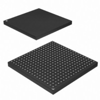
AT91SAM9263B-CU Atmel, AT91SAM9263B-CU Datasheet - Page 806

AT91SAM9263B-CU
Manufacturer Part Number
AT91SAM9263B-CU
Description
IC ARM9 MCU 200 MHZ 324-TFBGA
Manufacturer
Atmel
Series
AT91SAMr
Specifications of AT91SAM9263B-CU
Core Processor
ARM9
Core Size
16/32-Bit
Speed
240MHz
Connectivity
CAN, Ethernet, I²C, MMC, SPI, SSC, UART/USART, USB
Peripherals
AC'97, LCD, POR, PWM, WDT
Number Of I /o
160
Program Memory Size
128KB (128K x 8)
Program Memory Type
ROM
Ram Size
128K x 8
Voltage - Supply (vcc/vdd)
1.08 V ~ 1.32 V
Oscillator Type
Internal
Operating Temperature
-40°C ~ 85°C
Package / Case
324-TFBGA
Processor Series
AT91SAMx
Core
ARM926EJ-S
Data Bus Width
32 bit
Data Ram Size
96 KB
Interface Type
2-Wire, EBI, I2S, MCI, SPI, USART
Maximum Clock Frequency
200 MHz
Number Of Programmable I/os
160
Number Of Timers
4
Maximum Operating Temperature
+ 85 C
Mounting Style
SMD/SMT
3rd Party Development Tools
JTRACE-ARM-2M, MDK-ARM, RL-ARM, ULINK2
Development Tools By Supplier
AT91SAM-ICE, AT91-ISP, AT91SAM9263-EK
Minimum Operating Temperature
- 40 C
Package
324TFBGA
Device Core
ARM926EJ-S
Family Name
91S
Maximum Speed
200 MHz
Operating Supply Voltage
1.8|2.5|3.3 V
Controller Family/series
AT91SAM9xxx
No. Of I/o's
160
Ram Memory Size
96KB
Cpu Speed
240MHz
No. Of Timers
1
Rohs Compliant
Yes
For Use With
AT91SAM9263-EK - KIT EVAL FOR AT91SAM9263AT91SAM-ICE - EMULATOR FOR AT91 ARM7/ARM9
Lead Free Status / RoHS Status
Lead free / RoHS Compliant
Eeprom Size
-
Data Converters
-
Lead Free Status / Rohs Status
Lead free / RoHS Compliant
Other names
Q3735625
Available stocks
Company
Part Number
Manufacturer
Quantity
Price
Company:
Part Number:
AT91SAM9263B-CU
Manufacturer:
IDT
Quantity:
1 043
Part Number:
AT91SAM9263B-CU
Manufacturer:
ATMEL/爱特梅尔
Quantity:
20 000
Company:
Part Number:
AT91SAM9263B-CU-100
Manufacturer:
ATMEL
Quantity:
1 000
- Current page: 806 of 1110
- Download datasheet (17Mb)
Table 41-1.
806
Bit
19:17
13:12
11:0
29
28
27
26
25
24
23
22
21
20
16
15
14
AT91SAM9263
Unicast hash match
External address match
Reserved for future use
Specific address register 1 match
Specific address register 2 match
Specific address register 3 match
Specific address register 4 match
Type ID match
VLAN tag detected (i.e., type id of 0x8100)
Priority tag detected (i.e., type id of 0x8100 and null VLAN identifier)
VLAN priority (only valid if bit 21 is set)
Concatenation format indicator (CFI) bit (only valid if bit 21 is set)
End of frame - when set the buffer contains the end of a frame. If end of frame is not set, then the only other valid status
are bits 12, 13 and 14.
Start of frame - when set the buffer contains the start of a frame. If both bits 15 and 14 are set, then the buffer contains a
whole frame.
Receive buffer offset - indicates the number of bytes by which the data in the first buffer is offset from the word address.
Updated with the current values of the network configuration register. If jumbo frame mode is enabled through bit 3 of the
network configuration register, then bits 13:12 of the receive buffer descriptor entry are used to indicate bits 13:12 of the
frame length.
Length of frame including FCS (if selected). Bits 13:12 are also used if jumbo frame mode is selected.
Receive Buffer Descriptor Entry (Continued)
To receive frames, the buffer descriptors must be initialized by writing an appropriate address to
bits 31 to 2 in the first word of each list entry. Bit zero must be written with zero. Bit one is the
wrap bit and indicates the last entry in the list.
The start location of the receive buffer descriptor list must be written to the receive buffer queue
pointer register before setting the receive enable bit in the network control register to enable
receive. As soon as the receive block starts writing received frame data to the receive FIFO, the
receive buffer manager reads the first receive buffer location pointed to by the receive buffer
queue pointer register.
If the filter block then indicates that the frame should be copied to memory, the receive data
DMA operation starts writing data into the receive buffer. If an error occurs, the buffer is recov-
ered. If the current buffer pointer has its wrap bit set or is the 1024
buffer location is read from the beginning of the receive descriptor list. Otherwise, the next
receive buffer location is read from the next word in memory.
There is an 11-bit counter to count out the 2048 word locations of a maximum length, receive
buffer descriptor list. This is added with the value originally written to the receive buffer queue
pointer register to produce a pointer into the list. A read of the receive buffer queue pointer reg-
ister returns the pointer value, which is the queue entry currently being accessed. The counter is
reset after receive status is written to a descriptor that has its wrap bit set or rolls over to zero
after 1024 descriptors have been accessed. The value written to the receive buffer pointer regis-
Function
th
descriptor, the next receive
6249H–ATARM–27-Jul-09
Related parts for AT91SAM9263B-CU
Image
Part Number
Description
Manufacturer
Datasheet
Request
R

Part Number:
Description:
MCU, MPU & DSP Development Tools KICKSTART KIT FOR AT91SAM9 PLUS
Manufacturer:
IAR Systems

Part Number:
Description:
DEV KIT FOR AVR/AVR32
Manufacturer:
Atmel
Datasheet:

Part Number:
Description:
INTERVAL AND WIPE/WASH WIPER CONTROL IC WITH DELAY
Manufacturer:
ATMEL Corporation
Datasheet:

Part Number:
Description:
Low-Voltage Voice-Switched IC for Hands-Free Operation
Manufacturer:
ATMEL Corporation
Datasheet:

Part Number:
Description:
MONOLITHIC INTEGRATED FEATUREPHONE CIRCUIT
Manufacturer:
ATMEL Corporation
Datasheet:

Part Number:
Description:
AM-FM Receiver IC U4255BM-M
Manufacturer:
ATMEL Corporation
Datasheet:

Part Number:
Description:
Monolithic Integrated Feature Phone Circuit
Manufacturer:
ATMEL Corporation
Datasheet:

Part Number:
Description:
Multistandard Video-IF and Quasi Parallel Sound Processing
Manufacturer:
ATMEL Corporation
Datasheet:

Part Number:
Description:
High-performance EE PLD
Manufacturer:
ATMEL Corporation
Datasheet:

Part Number:
Description:
8-bit Flash Microcontroller
Manufacturer:
ATMEL Corporation
Datasheet:

Part Number:
Description:
2-Wire Serial EEPROM
Manufacturer:
ATMEL Corporation
Datasheet:


