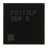
DF2117VLP20V Renesas Electronics America, DF2117VLP20V Datasheet - Page 807

DF2117VLP20V
Manufacturer Part Number
DF2117VLP20V
Description
IC H8S/2117 MCU FLASH 145TFLGA
Manufacturer
Renesas Electronics America
Series
H8® H8S/2100r
Datasheet
1.DF2117VBG20V.pdf
(960 pages)
Specifications of DF2117VLP20V
Core Processor
H8S/2600
Core Size
16-Bit
Speed
20MHz
Connectivity
FIFO, I²C, LPC, SCI, SmartCard
Peripherals
POR, PWM, WDT
Number Of I /o
112
Program Memory Size
160KB (160K x 8)
Program Memory Type
FLASH
Ram Size
8K x 8
Voltage - Supply (vcc/vdd)
3 V ~ 3.6 V
Data Converters
A/D 16x10b
Oscillator Type
External
Operating Temperature
-20°C ~ 75°C
Package / Case
145-TFLGA
For Use With
HS0005KCU11H - EMULATOR E10A-USB H8S(X),SH2(A)3DK2166 - DEV EVAL KIT H8S/2166
Lead Free Status / RoHS Status
Lead free / RoHS Compliant
Eeprom Size
-
Available stocks
Company
Part Number
Manufacturer
Quantity
Price
Company:
Part Number:
DF2117VLP20V
Manufacturer:
Renesas
Quantity:
100
Part Number:
DF2117VLP20V
Manufacturer:
RENESAS/瑞萨
Quantity:
20 000
- Current page: 807 of 960
- Download datasheet (6Mb)
Table 23.2 Crystal Resonator Parameters
23.1.2
Figure 23.4 shows a typical method of inputting an external clock signal. To leave the XTAL pin
open, incidental capacitance should be 10 pF or less. To input an inverted clock to the XTAL pin,
the external clock should be set to high in standby mode or watch mode. External clock input
conditions are shown in table 23.3. The frequency of the external clock should be the same as that
of the system clock (φ).
Frequency (MHz)
R
C
S
0
(max) (pF)
(max) (Ω)
External Clock Input Method
EXTAL
XTAL
EXTAL
XTAL
(a) Example of external clock input when XTAL pin is left open
(b) Example of external clock input when an inverted clock is input to XTAL pin
Figure 23.4 Example of External Clock Input
80
8
7
10
70
7
Open
External clock input
External clock input
12
60
Rev. 3.00 Sep. 28, 2009 Page 761 of 910
7
Section 23 Clock Pulse Generator
16
50
7
REJ09B0350-0300
40
20
7
Related parts for DF2117VLP20V
Image
Part Number
Description
Manufacturer
Datasheet
Request
R

Part Number:
Description:
KIT STARTER FOR M16C/29
Manufacturer:
Renesas Electronics America
Datasheet:

Part Number:
Description:
KIT STARTER FOR R8C/2D
Manufacturer:
Renesas Electronics America
Datasheet:

Part Number:
Description:
R0K33062P STARTER KIT
Manufacturer:
Renesas Electronics America
Datasheet:

Part Number:
Description:
KIT STARTER FOR R8C/23 E8A
Manufacturer:
Renesas Electronics America
Datasheet:

Part Number:
Description:
KIT STARTER FOR R8C/25
Manufacturer:
Renesas Electronics America
Datasheet:

Part Number:
Description:
KIT STARTER H8S2456 SHARPE DSPLY
Manufacturer:
Renesas Electronics America
Datasheet:

Part Number:
Description:
KIT STARTER FOR R8C38C
Manufacturer:
Renesas Electronics America
Datasheet:

Part Number:
Description:
KIT STARTER FOR R8C35C
Manufacturer:
Renesas Electronics America
Datasheet:

Part Number:
Description:
KIT STARTER FOR R8CL3AC+LCD APPS
Manufacturer:
Renesas Electronics America
Datasheet:

Part Number:
Description:
KIT STARTER FOR RX610
Manufacturer:
Renesas Electronics America
Datasheet:

Part Number:
Description:
KIT STARTER FOR R32C/118
Manufacturer:
Renesas Electronics America
Datasheet:

Part Number:
Description:
KIT DEV RSK-R8C/26-29
Manufacturer:
Renesas Electronics America
Datasheet:

Part Number:
Description:
KIT STARTER FOR SH7124
Manufacturer:
Renesas Electronics America
Datasheet:

Part Number:
Description:
KIT STARTER FOR H8SX/1622
Manufacturer:
Renesas Electronics America
Datasheet:

Part Number:
Description:
KIT DEV FOR SH7203
Manufacturer:
Renesas Electronics America
Datasheet:


