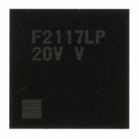
DF2117VLP20V Renesas Electronics America, DF2117VLP20V Datasheet - Page 638

DF2117VLP20V
Manufacturer Part Number
DF2117VLP20V
Description
IC H8S/2117 MCU FLASH 145TFLGA
Manufacturer
Renesas Electronics America
Series
H8® H8S/2100r
Datasheet
1.DF2117VBG20V.pdf
(960 pages)
Specifications of DF2117VLP20V
Core Processor
H8S/2600
Core Size
16-Bit
Speed
20MHz
Connectivity
FIFO, I²C, LPC, SCI, SmartCard
Peripherals
POR, PWM, WDT
Number Of I /o
112
Program Memory Size
160KB (160K x 8)
Program Memory Type
FLASH
Ram Size
8K x 8
Voltage - Supply (vcc/vdd)
3 V ~ 3.6 V
Data Converters
A/D 16x10b
Oscillator Type
External
Operating Temperature
-20°C ~ 75°C
Package / Case
145-TFLGA
For Use With
HS0005KCU11H - EMULATOR E10A-USB H8S(X),SH2(A)3DK2166 - DEV EVAL KIT H8S/2166
Lead Free Status / RoHS Status
Lead free / RoHS Compliant
Eeprom Size
-
Available stocks
Company
Part Number
Manufacturer
Quantity
Price
Company:
Part Number:
DF2117VLP20V
Manufacturer:
Renesas
Quantity:
100
Part Number:
DF2117VLP20V
Manufacturer:
RENESAS/瑞萨
Quantity:
20 000
- Current page: 638 of 960
- Download datasheet (6Mb)
Section 19 LPC Interface (LPC)
19.2
Table 19.1 lists the LPC pin configuration.
Table 19.1 Pin Configuration
Notes: 1. Pin state monitoring input is possible in addition to the LPC interface control
Rev. 3.00 Sep. 28, 2009 Page 592 of 910
REJ09B0350-0300
Name
LPC address/
data 3 to 0
LPC frame
LPC reset
LPC clock
Serialized
interrupt request
LSCI general
output
LSMI general
output
PME general
output
GATE A20
LPC clock run
LPC power-down LPCPD
2. Only 0 can be output. If 1 is output, the pin is in the high-impedance state, so an
Input/Output Pins
input/output function.
external resistor is necessary to pull the signal up to VCC.
Abbreviation
LAD3 to LAD0 P33 to P30 I/O
LFRAME
LRESET
LCLK
SERIRQ
LSCI
LSMI
PME
GA20
CLKRUN
Port
P34
P35
P36
P37
PB1
PB0
P80
P81
P82
P83
I/O
Input*
Input*
Input
I/O*
Output*
Output*
Output*
Output*
I/O*
Input*
1
1,
*
1
1
1
2
1,
1,
1,
1,
*
*
*
*
2
2
2
2
Function
Cycle type/address/data signals
serially (4-signal-line) transferred in
synchronization with LCLK
Transfer cycle start and forced
termination signal
LPC interface reset signal
33-MHz PCI clock signal
Serialized host interrupt request
signal in synchronization with LCLK
General output
General output
General output
Gate A20 control signal output
LCLK restart request signal when
serial host interrupt is requested
LPC module shutdown signal
Related parts for DF2117VLP20V
Image
Part Number
Description
Manufacturer
Datasheet
Request
R

Part Number:
Description:
KIT STARTER FOR M16C/29
Manufacturer:
Renesas Electronics America
Datasheet:

Part Number:
Description:
KIT STARTER FOR R8C/2D
Manufacturer:
Renesas Electronics America
Datasheet:

Part Number:
Description:
R0K33062P STARTER KIT
Manufacturer:
Renesas Electronics America
Datasheet:

Part Number:
Description:
KIT STARTER FOR R8C/23 E8A
Manufacturer:
Renesas Electronics America
Datasheet:

Part Number:
Description:
KIT STARTER FOR R8C/25
Manufacturer:
Renesas Electronics America
Datasheet:

Part Number:
Description:
KIT STARTER H8S2456 SHARPE DSPLY
Manufacturer:
Renesas Electronics America
Datasheet:

Part Number:
Description:
KIT STARTER FOR R8C38C
Manufacturer:
Renesas Electronics America
Datasheet:

Part Number:
Description:
KIT STARTER FOR R8C35C
Manufacturer:
Renesas Electronics America
Datasheet:

Part Number:
Description:
KIT STARTER FOR R8CL3AC+LCD APPS
Manufacturer:
Renesas Electronics America
Datasheet:

Part Number:
Description:
KIT STARTER FOR RX610
Manufacturer:
Renesas Electronics America
Datasheet:

Part Number:
Description:
KIT STARTER FOR R32C/118
Manufacturer:
Renesas Electronics America
Datasheet:

Part Number:
Description:
KIT DEV RSK-R8C/26-29
Manufacturer:
Renesas Electronics America
Datasheet:

Part Number:
Description:
KIT STARTER FOR SH7124
Manufacturer:
Renesas Electronics America
Datasheet:

Part Number:
Description:
KIT STARTER FOR H8SX/1622
Manufacturer:
Renesas Electronics America
Datasheet:

Part Number:
Description:
KIT DEV FOR SH7203
Manufacturer:
Renesas Electronics America
Datasheet:


