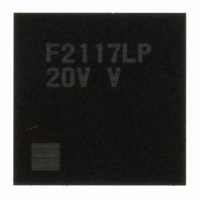
DF2117VLP20V Renesas Electronics America, DF2117VLP20V Datasheet - Page 748

DF2117VLP20V
Manufacturer Part Number
DF2117VLP20V
Description
IC H8S/2117 MCU FLASH 145TFLGA
Manufacturer
Renesas Electronics America
Series
H8® H8S/2100r
Datasheet
1.DF2117VBG20V.pdf
(960 pages)
Specifications of DF2117VLP20V
Core Processor
H8S/2600
Core Size
16-Bit
Speed
20MHz
Connectivity
FIFO, I²C, LPC, SCI, SmartCard
Peripherals
POR, PWM, WDT
Number Of I /o
112
Program Memory Size
160KB (160K x 8)
Program Memory Type
FLASH
Ram Size
8K x 8
Voltage - Supply (vcc/vdd)
3 V ~ 3.6 V
Data Converters
A/D 16x10b
Oscillator Type
External
Operating Temperature
-20°C ~ 75°C
Package / Case
145-TFLGA
For Use With
HS0005KCU11H - EMULATOR E10A-USB H8S(X),SH2(A)3DK2166 - DEV EVAL KIT H8S/2166
Lead Free Status / RoHS Status
Lead free / RoHS Compliant
Eeprom Size
-
Available stocks
Company
Part Number
Manufacturer
Quantity
Price
Company:
Part Number:
DF2117VLP20V
Manufacturer:
Renesas
Quantity:
100
Part Number:
DF2117VLP20V
Manufacturer:
RENESAS/瑞萨
Quantity:
20 000
- Current page: 748 of 960
- Download datasheet (6Mb)
Section 22 Flash Memory
22.8.1
Boot mode executes programming/erasing of the user MAT and the user boot MAT by means of
the control command and program data transmitted from the externally connected host via the on-
chip SCI_1.
In boot mode, the tool for transmitting the control command and program data, and the program
data must be prepared in the host. The serial communication mode is set to asynchronous mode.
The system configuration in boot mode is shown in figure 22.6. Interrupts are ignored in boot
mode. Configure the user system so that interrupts do not occur.
(1)
The SCI_1 is set to asynchronous mode, and the serial transmit/receive format is set to 8-bit data,
one stop bit, and no parity.
When a transition to boot mode is made, the boot program embedded in this LSI is initiated.
When the boot program is initiated, this LSI measures the low period of asynchronous serial
communication data (H'00) transmitted consecutively by the host, calculates the bit rate, and
adjusts the bit rate of the SCI_1 to match that of the host.
When bit rate adjustment is completed, this LSI transmits 1 byte of H'00 to the host as the bit
adjustment end sign. When the host receives this bit adjustment end sign normally, it transmits 1
byte of H'55 to this LSI. When reception is not executed normally, initiate boot mode again. The
bit rate may not be adjusted within the allowable range depending on the combination of the bit
rate of the host and the system clock frequency of this LSI. Therefore, the transfer bit rate of the
host and the system clock frequency of this LSI must be as shown in table 22.8.
Rev. 3.00 Sep. 28, 2009 Page 702 of 910
REJ09B0350-0300
Serial Interface Setting by Host
Boot Mode
tool and program
Programming
Host
data
Figure 22.6 System Configuration in Boot Mode
Control command,
program data
Response
RxD1
TxD1
Software for
analyzing
control
commands
(on-chip)
SCI_1
This LSI
On-chip
memory
Flash
RAM
Related parts for DF2117VLP20V
Image
Part Number
Description
Manufacturer
Datasheet
Request
R

Part Number:
Description:
KIT STARTER FOR M16C/29
Manufacturer:
Renesas Electronics America
Datasheet:

Part Number:
Description:
KIT STARTER FOR R8C/2D
Manufacturer:
Renesas Electronics America
Datasheet:

Part Number:
Description:
R0K33062P STARTER KIT
Manufacturer:
Renesas Electronics America
Datasheet:

Part Number:
Description:
KIT STARTER FOR R8C/23 E8A
Manufacturer:
Renesas Electronics America
Datasheet:

Part Number:
Description:
KIT STARTER FOR R8C/25
Manufacturer:
Renesas Electronics America
Datasheet:

Part Number:
Description:
KIT STARTER H8S2456 SHARPE DSPLY
Manufacturer:
Renesas Electronics America
Datasheet:

Part Number:
Description:
KIT STARTER FOR R8C38C
Manufacturer:
Renesas Electronics America
Datasheet:

Part Number:
Description:
KIT STARTER FOR R8C35C
Manufacturer:
Renesas Electronics America
Datasheet:

Part Number:
Description:
KIT STARTER FOR R8CL3AC+LCD APPS
Manufacturer:
Renesas Electronics America
Datasheet:

Part Number:
Description:
KIT STARTER FOR RX610
Manufacturer:
Renesas Electronics America
Datasheet:

Part Number:
Description:
KIT STARTER FOR R32C/118
Manufacturer:
Renesas Electronics America
Datasheet:

Part Number:
Description:
KIT DEV RSK-R8C/26-29
Manufacturer:
Renesas Electronics America
Datasheet:

Part Number:
Description:
KIT STARTER FOR SH7124
Manufacturer:
Renesas Electronics America
Datasheet:

Part Number:
Description:
KIT STARTER FOR H8SX/1622
Manufacturer:
Renesas Electronics America
Datasheet:

Part Number:
Description:
KIT DEV FOR SH7203
Manufacturer:
Renesas Electronics America
Datasheet:


