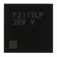
DF2117VLP20V Renesas Electronics America, DF2117VLP20V Datasheet - Page 751

DF2117VLP20V
Manufacturer Part Number
DF2117VLP20V
Description
IC H8S/2117 MCU FLASH 145TFLGA
Manufacturer
Renesas Electronics America
Series
H8® H8S/2100r
Datasheet
1.DF2117VBG20V.pdf
(960 pages)
Specifications of DF2117VLP20V
Core Processor
H8S/2600
Core Size
16-Bit
Speed
20MHz
Connectivity
FIFO, I²C, LPC, SCI, SmartCard
Peripherals
POR, PWM, WDT
Number Of I /o
112
Program Memory Size
160KB (160K x 8)
Program Memory Type
FLASH
Ram Size
8K x 8
Voltage - Supply (vcc/vdd)
3 V ~ 3.6 V
Data Converters
A/D 16x10b
Oscillator Type
External
Operating Temperature
-20°C ~ 75°C
Package / Case
145-TFLGA
For Use With
HS0005KCU11H - EMULATOR E10A-USB H8S(X),SH2(A)3DK2166 - DEV EVAL KIT H8S/2166
Lead Free Status / RoHS Status
Lead free / RoHS Compliant
Eeprom Size
-
Available stocks
Company
Part Number
Manufacturer
Quantity
Price
Company:
Part Number:
DF2117VLP20V
Manufacturer:
Renesas
Quantity:
100
Part Number:
DF2117VLP20V
Manufacturer:
RENESAS/瑞萨
Quantity:
20 000
- Current page: 751 of 960
- Download datasheet (6Mb)
4. When the program preparation notice is received, the state of waiting for program data is
Memory read of the user MAT and user boot MAT can only read the data programmed after all
user MAT and user boot MAT have automatically been erased. No other data can be read.
entered. The start address of the programming destination and program data must be
transmitted after the programming command is transmitted. When programming is finished,
the start address of the programming destination must be set to H'FFFFFFFF and transmitted.
Then the state of waiting for program data is returned to the state of waiting for
programming/erasing command. When reprogramming an erase block including an area on
which the programming end command is issued, erase the erase block. An example of the
erase block is shown in figure 22.9. When the erasure preparation notice is received, the state
of waiting for erase block data is entered. The erase block number must be transmitted after the
erasing command is transmitted. When the erasure is finished, the erase block number must be
set to H'FF and transmitted. Then the state of waiting for erase block data is returned to the
state of waiting for programming/erasing command. Erasure must be executed when the
specified block is programmed without a reset start after programming is executed in boot
mode. When programming can be executed by only one operation, all blocks are erased before
entering the state of waiting for programming/erasing command or another command. Thus, in
this case, the erasing operation is not required. The commands other than the
programming/erasing command perform sum check, blank check (erasure check), and memory
read of the user MAT and user boot MAT, and acquisition of current status information.
Figure 22.9 Example of Erase Block Including Programmed Area
Programming
end area
EB5
EB6
EB7
EB8
Before reprogramming erase blocks EB6 and
EB7 on which the programming end command
is issued, erase the blocks (EB6 and EB7).
Rev. 3.00 Sep. 28, 2009 Page 705 of 910
Section 22 Flash Memory
REJ09B0350-0300
Related parts for DF2117VLP20V
Image
Part Number
Description
Manufacturer
Datasheet
Request
R

Part Number:
Description:
KIT STARTER FOR M16C/29
Manufacturer:
Renesas Electronics America
Datasheet:

Part Number:
Description:
KIT STARTER FOR R8C/2D
Manufacturer:
Renesas Electronics America
Datasheet:

Part Number:
Description:
R0K33062P STARTER KIT
Manufacturer:
Renesas Electronics America
Datasheet:

Part Number:
Description:
KIT STARTER FOR R8C/23 E8A
Manufacturer:
Renesas Electronics America
Datasheet:

Part Number:
Description:
KIT STARTER FOR R8C/25
Manufacturer:
Renesas Electronics America
Datasheet:

Part Number:
Description:
KIT STARTER H8S2456 SHARPE DSPLY
Manufacturer:
Renesas Electronics America
Datasheet:

Part Number:
Description:
KIT STARTER FOR R8C38C
Manufacturer:
Renesas Electronics America
Datasheet:

Part Number:
Description:
KIT STARTER FOR R8C35C
Manufacturer:
Renesas Electronics America
Datasheet:

Part Number:
Description:
KIT STARTER FOR R8CL3AC+LCD APPS
Manufacturer:
Renesas Electronics America
Datasheet:

Part Number:
Description:
KIT STARTER FOR RX610
Manufacturer:
Renesas Electronics America
Datasheet:

Part Number:
Description:
KIT STARTER FOR R32C/118
Manufacturer:
Renesas Electronics America
Datasheet:

Part Number:
Description:
KIT DEV RSK-R8C/26-29
Manufacturer:
Renesas Electronics America
Datasheet:

Part Number:
Description:
KIT STARTER FOR SH7124
Manufacturer:
Renesas Electronics America
Datasheet:

Part Number:
Description:
KIT STARTER FOR H8SX/1622
Manufacturer:
Renesas Electronics America
Datasheet:

Part Number:
Description:
KIT DEV FOR SH7203
Manufacturer:
Renesas Electronics America
Datasheet:


