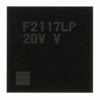
DF2117VLP20V Renesas Electronics America, DF2117VLP20V Datasheet - Page 24

DF2117VLP20V
Manufacturer Part Number
DF2117VLP20V
Description
IC H8S/2117 MCU FLASH 145TFLGA
Manufacturer
Renesas Electronics America
Series
H8® H8S/2100r
Datasheet
1.DF2117VBG20V.pdf
(960 pages)
Specifications of DF2117VLP20V
Core Processor
H8S/2600
Core Size
16-Bit
Speed
20MHz
Connectivity
FIFO, I²C, LPC, SCI, SmartCard
Peripherals
POR, PWM, WDT
Number Of I /o
112
Program Memory Size
160KB (160K x 8)
Program Memory Type
FLASH
Ram Size
8K x 8
Voltage - Supply (vcc/vdd)
3 V ~ 3.6 V
Data Converters
A/D 16x10b
Oscillator Type
External
Operating Temperature
-20°C ~ 75°C
Package / Case
145-TFLGA
For Use With
HS0005KCU11H - EMULATOR E10A-USB H8S(X),SH2(A)3DK2166 - DEV EVAL KIT H8S/2166
Lead Free Status / RoHS Status
Lead free / RoHS Compliant
Eeprom Size
-
Available stocks
Company
Part Number
Manufacturer
Quantity
Price
Company:
Part Number:
DF2117VLP20V
Manufacturer:
Renesas
Quantity:
100
Part Number:
DF2117VLP20V
Manufacturer:
RENESAS/瑞萨
Quantity:
20 000
- Current page: 24 of 960
- Download datasheet (6Mb)
Rev. 3.00 Sep. 28, 2009 Page xxii of xliv
REJ09B0350-0300
Item
22.8.4 Storable Areas for On-
Chip Program and Program Data
Table 22.10 Usable Area for
Programming in User Program
Mode
Table 22.11 Usable Area for
Erasure in User Program Mode
Table 22.12 Usable Area for
Programming in User Boot Mode
Table 22.13 Usable Area for
Erasure in User Boot Mode
22.11 Programmer Mode
Table 22.16 Device Types
Supported in Programmer Mode
22.12 Standard Serial
Communication Interface
Specifications for Boot Mode
Page Revision (See Manual for Details)
720
721
722
723
728
728
Table amended
Table amended
Table added
Table added
Table amended
Note amended
Note: * For the R4F2117 model, 160 kbytes of ROM
Description amended
2. Inquiry/selection state
Item
Operation for initialization error
Operation for disabling interrupts
Item
Operation for initialization error
Operation for disabling interrupts
Target Memory MAT
User MAT
User boot MAT
In this state, the boot program responds to inquiry
commands from the host. The device name, clock
mode, and bit rate are selected. After selection of
these settings, the program is made to enter the
programming/erasing state by the command for a
transition to the programming/erasing state. The
program transfers the libraries required for erasure
to the on-chip RAM and erases the user MATs and
user boot MATs before the transition.
space is available when the user MAT is
selected. If programming is performed in
programmer mode, H'FF data must be written
to address H'28000 to H'3FFFF with 256-kbyte
capacity setting.
R/W
256 kbytes*
8 kbytes
Storable/Executable Area
On-Chip RAM
O
O
Storable/Executable Area
On-Chip RAM
O
O
User MAT
O
O
User MAT
O
O
Description
FZTAT256V3A
FZTATUSBTV3A
Selected MAT
User MAT
O
O
Selected MAT
User MAT
O
O
Embedded
Program
Storage MAT
Embedded
Program
Storage MAT
Related parts for DF2117VLP20V
Image
Part Number
Description
Manufacturer
Datasheet
Request
R

Part Number:
Description:
KIT STARTER FOR M16C/29
Manufacturer:
Renesas Electronics America
Datasheet:

Part Number:
Description:
KIT STARTER FOR R8C/2D
Manufacturer:
Renesas Electronics America
Datasheet:

Part Number:
Description:
R0K33062P STARTER KIT
Manufacturer:
Renesas Electronics America
Datasheet:

Part Number:
Description:
KIT STARTER FOR R8C/23 E8A
Manufacturer:
Renesas Electronics America
Datasheet:

Part Number:
Description:
KIT STARTER FOR R8C/25
Manufacturer:
Renesas Electronics America
Datasheet:

Part Number:
Description:
KIT STARTER H8S2456 SHARPE DSPLY
Manufacturer:
Renesas Electronics America
Datasheet:

Part Number:
Description:
KIT STARTER FOR R8C38C
Manufacturer:
Renesas Electronics America
Datasheet:

Part Number:
Description:
KIT STARTER FOR R8C35C
Manufacturer:
Renesas Electronics America
Datasheet:

Part Number:
Description:
KIT STARTER FOR R8CL3AC+LCD APPS
Manufacturer:
Renesas Electronics America
Datasheet:

Part Number:
Description:
KIT STARTER FOR RX610
Manufacturer:
Renesas Electronics America
Datasheet:

Part Number:
Description:
KIT STARTER FOR R32C/118
Manufacturer:
Renesas Electronics America
Datasheet:

Part Number:
Description:
KIT DEV RSK-R8C/26-29
Manufacturer:
Renesas Electronics America
Datasheet:

Part Number:
Description:
KIT STARTER FOR SH7124
Manufacturer:
Renesas Electronics America
Datasheet:

Part Number:
Description:
KIT STARTER FOR H8SX/1622
Manufacturer:
Renesas Electronics America
Datasheet:

Part Number:
Description:
KIT DEV FOR SH7203
Manufacturer:
Renesas Electronics America
Datasheet:


