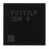
DF2117VLP20V Renesas Electronics America, DF2117VLP20V Datasheet - Page 497

DF2117VLP20V
Manufacturer Part Number
DF2117VLP20V
Description
IC H8S/2117 MCU FLASH 145TFLGA
Manufacturer
Renesas Electronics America
Series
H8® H8S/2100r
Datasheet
1.DF2117VBG20V.pdf
(960 pages)
Specifications of DF2117VLP20V
Core Processor
H8S/2600
Core Size
16-Bit
Speed
20MHz
Connectivity
FIFO, I²C, LPC, SCI, SmartCard
Peripherals
POR, PWM, WDT
Number Of I /o
112
Program Memory Size
160KB (160K x 8)
Program Memory Type
FLASH
Ram Size
8K x 8
Voltage - Supply (vcc/vdd)
3 V ~ 3.6 V
Data Converters
A/D 16x10b
Oscillator Type
External
Operating Temperature
-20°C ~ 75°C
Package / Case
145-TFLGA
For Use With
HS0005KCU11H - EMULATOR E10A-USB H8S(X),SH2(A)3DK2166 - DEV EVAL KIT H8S/2166
Lead Free Status / RoHS Status
Lead free / RoHS Compliant
Eeprom Size
-
Available stocks
Company
Part Number
Manufacturer
Quantity
Price
Company:
Part Number:
DF2117VLP20V
Manufacturer:
Renesas
Quantity:
100
Part Number:
DF2117VLP20V
Manufacturer:
RENESAS/瑞萨
Quantity:
20 000
- Current page: 497 of 960
- Download datasheet (6Mb)
15.7.4
Only the internal clock generated by the internal baud rate generator can be used as a
communication clock in smart card interface mode. In this mode, the SCI can operate using a
basic clock with a frequency of 32, 64, 372, or 256 times the bit rate according to the BCP1 and
BCP0 settings (the frequency is always 16 times the bit rate in normal asynchronous mode). At
reception, the falling edge of the start bit is sampled using the internal basic clock in order to
perform internal synchronization. Receive data is sampled at the 16th, 32nd, 186th and 128th
rising edges of the basic clock pulses so that it can be latched at the center of each bit as shown in
figure 15.25. The reception margin here is determined by the following formula.
Assuming values of F = 0, D = 0.5, and N = 372 in formula (1), the reception margin is
determined by the formula below.
Internal
basic clock
Receive data
(RxD)
Synchronization
sampling timing
Data sampling
timing
Figure 15.25 Receive Data Sampling Timing in Smart Card Interface Mode
M = ⏐ (0.5 –
M = (0.5 – 1 / 2 × 372) × 100 [%] = 49.866%
M: Reception margin (%)
N: Ratio of bit rate to clock (N = 32, 64, 372, 256)
D: Clock duty (D = 0 to 1.0)
L: Frame length (L = 10)
F: Absolute value of clock rate deviation
Receive Data Sampling Timing and Reception Margin
(When Clock Frequency is 372 Times the Bit Rate)
2N
1
0
186 clock
) – (L – 0.5) F –
cycles
372 clock cycles
185
Start bit
371
⏐ D – 0.5 ⏐
0
N
D0
Section 15 Serial Communication Interface (SCI)
(1 + F) ⏐ × 100 [%]
Rev. 3.00 Sep. 28, 2009 Page 451 of 910
185
371 0
... Formula (1)
REJ09B0350-0300
D1
Related parts for DF2117VLP20V
Image
Part Number
Description
Manufacturer
Datasheet
Request
R

Part Number:
Description:
KIT STARTER FOR M16C/29
Manufacturer:
Renesas Electronics America
Datasheet:

Part Number:
Description:
KIT STARTER FOR R8C/2D
Manufacturer:
Renesas Electronics America
Datasheet:

Part Number:
Description:
R0K33062P STARTER KIT
Manufacturer:
Renesas Electronics America
Datasheet:

Part Number:
Description:
KIT STARTER FOR R8C/23 E8A
Manufacturer:
Renesas Electronics America
Datasheet:

Part Number:
Description:
KIT STARTER FOR R8C/25
Manufacturer:
Renesas Electronics America
Datasheet:

Part Number:
Description:
KIT STARTER H8S2456 SHARPE DSPLY
Manufacturer:
Renesas Electronics America
Datasheet:

Part Number:
Description:
KIT STARTER FOR R8C38C
Manufacturer:
Renesas Electronics America
Datasheet:

Part Number:
Description:
KIT STARTER FOR R8C35C
Manufacturer:
Renesas Electronics America
Datasheet:

Part Number:
Description:
KIT STARTER FOR R8CL3AC+LCD APPS
Manufacturer:
Renesas Electronics America
Datasheet:

Part Number:
Description:
KIT STARTER FOR RX610
Manufacturer:
Renesas Electronics America
Datasheet:

Part Number:
Description:
KIT STARTER FOR R32C/118
Manufacturer:
Renesas Electronics America
Datasheet:

Part Number:
Description:
KIT DEV RSK-R8C/26-29
Manufacturer:
Renesas Electronics America
Datasheet:

Part Number:
Description:
KIT STARTER FOR SH7124
Manufacturer:
Renesas Electronics America
Datasheet:

Part Number:
Description:
KIT STARTER FOR H8SX/1622
Manufacturer:
Renesas Electronics America
Datasheet:

Part Number:
Description:
KIT DEV FOR SH7203
Manufacturer:
Renesas Electronics America
Datasheet:


