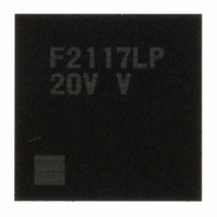
DF2117VLP20V Renesas Electronics America, DF2117VLP20V Datasheet - Page 70

DF2117VLP20V
Manufacturer Part Number
DF2117VLP20V
Description
IC H8S/2117 MCU FLASH 145TFLGA
Manufacturer
Renesas Electronics America
Series
H8® H8S/2100r
Datasheet
1.DF2117VBG20V.pdf
(960 pages)
Specifications of DF2117VLP20V
Core Processor
H8S/2600
Core Size
16-Bit
Speed
20MHz
Connectivity
FIFO, I²C, LPC, SCI, SmartCard
Peripherals
POR, PWM, WDT
Number Of I /o
112
Program Memory Size
160KB (160K x 8)
Program Memory Type
FLASH
Ram Size
8K x 8
Voltage - Supply (vcc/vdd)
3 V ~ 3.6 V
Data Converters
A/D 16x10b
Oscillator Type
External
Operating Temperature
-20°C ~ 75°C
Package / Case
145-TFLGA
For Use With
HS0005KCU11H - EMULATOR E10A-USB H8S(X),SH2(A)3DK2166 - DEV EVAL KIT H8S/2166
Lead Free Status / RoHS Status
Lead free / RoHS Compliant
Eeprom Size
-
Available stocks
Company
Part Number
Manufacturer
Quantity
Price
Company:
Part Number:
DF2117VLP20V
Manufacturer:
Renesas
Quantity:
100
Part Number:
DF2117VLP20V
Manufacturer:
RENESAS/瑞萨
Quantity:
20 000
- Current page: 70 of 960
- Download datasheet (6Mb)
Section 1 Overview
Rev. 3.00 Sep. 28, 2009 Page 24 of 910
REJ09B0350-0300
Type
A/D
converter
I
interface
(IIC)
2
C bus
Symbol
AN15 to
AN0
AVCC
AVref
AVSS
SCL0
SCL1
SCL2
ExSCLA
ExSCLB
SDA0
SDA1
SDA2
ExSDAA
ExSDAB
59 to 66,
75 to 68
76
77
67
14
135
55
53
51
17
138
56
54
52
TFP-144V BP-176V TLP-145V I/O
M10, N10,
R10, P10,
N11, R11,
P11, M11,
P15, N13,
R15, P14,
R14, P13,
R13, N12
N14, N15 M12
M14, M15 L11
R12, P12
F2
B6
P8
M8
R7
G2
D5
N9
R8
P7
Pin No.
L7, K9,
N8, M9,
L8, K10,
N9, M10,
L12, N13,
M13, N12,
N11, L10,
M11, N10
L9
E4
C6
K7
N6
L6
F1
B4
K8
K6
M7
Input
Input/
Output
Input/
Output
Input
Input
Input
Analog input pins.
the A/D converter.
When the A/D converter is
not used, this pin should be
connected to the system
power supply (+3 V).
for the A/D converter.
When the A/D converter is
not used, this pin should be
connected to the system
power supply (+3 V).
Ground pin for the A/D
converter. This pin should be
connected to the system
power supply (0 V).
I
type is NMOS open-drain.
To which pin the clock is
input or output can be
selected from the SCL0,
SCL1, ExSCLA, and ExSCLB
pins.
I
type is NMOS open-drain.
To which pin the clock is
input or output can be
selected from the SDA0,
SDA1, ExSDAA, and
ExSDAB pins.
Name and Function
Analog power supply pin for
Reference power supply pin
2
2
C clock I/O pins. The output
C data I/O pins. The output
Related parts for DF2117VLP20V
Image
Part Number
Description
Manufacturer
Datasheet
Request
R

Part Number:
Description:
KIT STARTER FOR M16C/29
Manufacturer:
Renesas Electronics America
Datasheet:

Part Number:
Description:
KIT STARTER FOR R8C/2D
Manufacturer:
Renesas Electronics America
Datasheet:

Part Number:
Description:
R0K33062P STARTER KIT
Manufacturer:
Renesas Electronics America
Datasheet:

Part Number:
Description:
KIT STARTER FOR R8C/23 E8A
Manufacturer:
Renesas Electronics America
Datasheet:

Part Number:
Description:
KIT STARTER FOR R8C/25
Manufacturer:
Renesas Electronics America
Datasheet:

Part Number:
Description:
KIT STARTER H8S2456 SHARPE DSPLY
Manufacturer:
Renesas Electronics America
Datasheet:

Part Number:
Description:
KIT STARTER FOR R8C38C
Manufacturer:
Renesas Electronics America
Datasheet:

Part Number:
Description:
KIT STARTER FOR R8C35C
Manufacturer:
Renesas Electronics America
Datasheet:

Part Number:
Description:
KIT STARTER FOR R8CL3AC+LCD APPS
Manufacturer:
Renesas Electronics America
Datasheet:

Part Number:
Description:
KIT STARTER FOR RX610
Manufacturer:
Renesas Electronics America
Datasheet:

Part Number:
Description:
KIT STARTER FOR R32C/118
Manufacturer:
Renesas Electronics America
Datasheet:

Part Number:
Description:
KIT DEV RSK-R8C/26-29
Manufacturer:
Renesas Electronics America
Datasheet:

Part Number:
Description:
KIT STARTER FOR SH7124
Manufacturer:
Renesas Electronics America
Datasheet:

Part Number:
Description:
KIT STARTER FOR H8SX/1622
Manufacturer:
Renesas Electronics America
Datasheet:

Part Number:
Description:
KIT DEV FOR SH7203
Manufacturer:
Renesas Electronics America
Datasheet:


