MOD5234-100IR NetBurner Inc, MOD5234-100IR Datasheet - Page 68
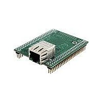
MOD5234-100IR
Manufacturer Part Number
MOD5234-100IR
Description
MOD5234 10/100 ETHERNET MODULE
Manufacturer
NetBurner Inc
Type
Controllers & Processorsr
Datasheets
1.MOD5272-100IR.pdf
(3 pages)
2.MOD5234-100IR.pdf
(4 pages)
3.MOD5234-100IR.pdf
(754 pages)
Specifications of MOD5234-100IR
Interface
I²C, SPI, UART
Voltage - Supply
2.5V
Mounting Type
Surface Mount
Package / Case
Module
Product
Modules
Lead Free Status / RoHS Status
Lead free / RoHS Compliant
Data Format
-
Baud Rates
-
Lead Free Status / Rohs Status
Lead free / RoHS Compliant
Other names
Q4483564


Signal Descriptions
2-10
Address Bus
Data Bus
Byte Strobes
Output Enable
Transfer Acknowledge
Transfer Error
Acknowledge
Read/Write
Transfer Size
Transfer Start
Signal Name
A[23:0]
D[31:0]
BS[3:0]
OE
TA
TEA
R/W
TSIZ[1:0]
TS
Abbreviation
Table 2-5. External Memory Interface Signals
MCF5235 Reference Manual, Rev. 2
The 24 dedicated address signals define the address of external byte,
word, and longword accesses. These three-state outputs are the 24
lsbs of the internal 32-bit address bus and multiplexed with the
SDRAM controller row and column addresses.
These three-state bidirectional signals provide the general purpose
data path between the processor and all other devices.
The D[15:0] pins can be configured as GPIO when using a 16-bit bus.
Define the flow of data on the data bus. During SRAM and peripheral
accesses, these output signals indicate that data is to be latched or
driven onto a byte of the data when driven low. The BS[3:0] signals are
asserted only to the memory bytes used during a read or write access.
BS0 controls access to the least significant byte lane of data, and BS3
controls access to the most significant byte lane of data.
The BS[3:0] signals are asserted during accesses to on-chip
peripherals but not to on-chip SRAM, or cache. During SDRAM
accesses, these signals act as the CAS[3:0] signals, which indicate a
byte transfers between SDRAM and the chip when driven high.
For SRAM or Flash devices, the BS[3:0] outputs should be connected
to individual byte strobe signals.
For SDRAM devices, the BS[3:0] should be connected to individual
SDRAM DQM signals. Note that most SDRAMs associate DQM3 with
the MSB, in which case BS3 should be connected to the SDRAM's
DQM3 input.
Indicates when an external device can drive data during external read
cycles.
Indicates that the external data transfer is complete. During a read
cycle, when the processor recognizes TA, it latches the data and then
terminates the bus cycle. During a write cycle, when the processor
recognizes TA, the bus cycle is terminated.
Indicates an error condition exists for the bus transfer. The bus cycle
is terminated and the CPU begins execution of the access error
exception.
Indicates the direction of the data transfer on the bus for SRAM (R/W)
and SDRAM (SD_WE) accesses. A logic 1 indicates a read from a
slave device and a logic 0 indicates a write to a slave device
When the device is in normal mode, static bus sizing lets the
programmer change data bus width between 8, 16, and 32 bits for
each chip select. The initial width for the bootstrap program chip
select, CS0, is determined by the state of TSIZ[1:0]. The program
should select bus widths for the other chip selects before accessing
the associated memory space. These pins arecxvvvvvvvvvvvvvvvvv
output pins.
Bus control output signal indicating the start of a transfer.
Function
Freescale Semiconductor
I/O
I/O
O
O
O
O
O
O
I
I
Related parts for MOD5234-100IR
Image
Part Number
Description
Manufacturer
Datasheet
Request
R

Part Number:
Description:
MCU, MPU & DSP Development Tools MOD5234 MODULE
Manufacturer:
NetBurner Inc
Datasheet:

Part Number:
Description:
MCU, MPU & DSP Development Tools MOD5234 Core Module Development Kit
Manufacturer:
NetBurner Inc
Datasheet:

Part Number:
Description:
BOARD SERIAL-ETHERNET 512K FLASH
Manufacturer:
NetBurner Inc
Datasheet:

Part Number:
Description:
PROCESSOR MODULE FLASH MOD5272
Manufacturer:
NetBurner Inc
Datasheet:

Part Number:
Description:
PROCESSOR MODULE 512KB FLASH
Manufacturer:
NetBurner Inc
Datasheet:

Part Number:
Description:
DUAL PORT SERIAL-ETHERNET
Manufacturer:
NetBurner Inc
Datasheet:

Part Number:
Description:
PROCESSOR MODULE FLASH
Manufacturer:
NetBurner Inc
Datasheet:

Part Number:
Description:
PROCESSOR MODULE 512KB FLASH
Manufacturer:
NetBurner Inc
Datasheet:

Part Number:
Description:
KIT DEVELOP NETWORK FOR MOD5282
Manufacturer:
NetBurner Inc
Datasheet:

Part Number:
Description:
KIT DEVELOP NETWORK FOR MOD5272
Manufacturer:
NetBurner Inc
Datasheet:

Part Number:
Description:
DUAL PORT SERIAL-ETHERNET
Manufacturer:
NetBurner Inc
Datasheet:

Part Number:
Description:
Ethernet Modules & Development Tools 32 Bit 66MHz 40 Pin DIP Industrial Temp
Manufacturer:
NetBurner Inc
Datasheet:

Part Number:
Description:
Ethernet ICs 32bit 147MHz CAN-to- Ethnt Device IndTemp
Manufacturer:
NetBurner Inc
Datasheet: