MOD5234-100IR NetBurner Inc, MOD5234-100IR Datasheet - Page 55
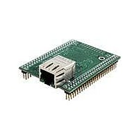
MOD5234-100IR
Manufacturer Part Number
MOD5234-100IR
Description
MOD5234 10/100 ETHERNET MODULE
Manufacturer
NetBurner Inc
Type
Controllers & Processorsr
Datasheets
1.MOD5272-100IR.pdf
(3 pages)
2.MOD5234-100IR.pdf
(4 pages)
3.MOD5234-100IR.pdf
(754 pages)
Specifications of MOD5234-100IR
Interface
I²C, SPI, UART
Voltage - Supply
2.5V
Mounting Type
Surface Mount
Package / Case
Module
Product
Modules
Lead Free Status / RoHS Status
Lead free / RoHS Compliant
Data Format
-
Baud Rates
-
Lead Free Status / Rohs Status
Lead free / RoHS Compliant
Other names
Q4483564


Features
1.3.16 Clock Module and Phase Locked Loop (PLL)
The clock module contains a crystal oscillator (OSC), phase-locked loop (PLL), reduced
frequency divider (RFD), status/control registers, and control logic. To improve noise immunity,
the PLL and OSC have their own power supply inputs, VDDPLL and VSSPLL. All other circuits
are powered by the normal supply pins, VDD, VSS, OVDD, and OVSS.
1.3.17 Interrupt Controllers (INTC0, INTC1)
There are two interrupt controllers on the MCF5235, each of which can support up to 63 interrupt
sources each for a total of 126. Each interrupt controller is organized as 7 levels with 9 interrupt
sources per level. Each interrupt source has a unique interrupt vector, and 56 of the 63 sources of
a given controller provide a programmable level [1-7] and priority within the level.
1.3.18 DMA Controller
The Direct Memory Access (DMA) Controller Module provides an efficient way to move blocks
of data with minimal processor interaction. The DMA module provides four channels
(DMA0-DMA3) that allow byte, word, longword or 16-byte burst line transfers. These transfers
are triggered by software explicitly setting a DCRn[START] bit. Other sources include the DMA
timer, external sources via the DREQ signal, and UARTs. The DMA controller supports dual
address to off-chip or on-chip devices.
1.3.19 External Interface Module (EIM)
The external bus interface handles the transfer of information between the core and memory,
peripherals, or other processing elements in the external address space. Features have been added
to support external Flash modules, for secondary wait states on reads and writes, and a signal to
support Active-Low Address Valid (a signal on most Flash memories).
Programmable chip-select outputs provide signals to enable external memory and peripheral
circuits, providing all handshaking and timing signals for automatic wait-state insertion and data
bus sizing.
Base memory address and block size are programmable, with some restrictions. For example, the
starting address must be on a boundary that is a multiple of the block size. Each chip select can be
configured to provide read and write enable signals suitable for use with most popular static RAMs
and peripherals. Data bus width (8-bit, 16-bit, or 32-bit) is programmable on all chip selects, and
further decoding is available for protection from read-only access.
MCF5235 Reference Manual, Rev. 2
Freescale Semiconductor
1-15
Related parts for MOD5234-100IR
Image
Part Number
Description
Manufacturer
Datasheet
Request
R

Part Number:
Description:
MCU, MPU & DSP Development Tools MOD5234 MODULE
Manufacturer:
NetBurner Inc
Datasheet:

Part Number:
Description:
MCU, MPU & DSP Development Tools MOD5234 Core Module Development Kit
Manufacturer:
NetBurner Inc
Datasheet:

Part Number:
Description:
BOARD SERIAL-ETHERNET 512K FLASH
Manufacturer:
NetBurner Inc
Datasheet:

Part Number:
Description:
PROCESSOR MODULE FLASH MOD5272
Manufacturer:
NetBurner Inc
Datasheet:

Part Number:
Description:
PROCESSOR MODULE 512KB FLASH
Manufacturer:
NetBurner Inc
Datasheet:

Part Number:
Description:
DUAL PORT SERIAL-ETHERNET
Manufacturer:
NetBurner Inc
Datasheet:

Part Number:
Description:
PROCESSOR MODULE FLASH
Manufacturer:
NetBurner Inc
Datasheet:

Part Number:
Description:
PROCESSOR MODULE 512KB FLASH
Manufacturer:
NetBurner Inc
Datasheet:

Part Number:
Description:
KIT DEVELOP NETWORK FOR MOD5282
Manufacturer:
NetBurner Inc
Datasheet:

Part Number:
Description:
KIT DEVELOP NETWORK FOR MOD5272
Manufacturer:
NetBurner Inc
Datasheet:

Part Number:
Description:
DUAL PORT SERIAL-ETHERNET
Manufacturer:
NetBurner Inc
Datasheet:

Part Number:
Description:
Ethernet Modules & Development Tools 32 Bit 66MHz 40 Pin DIP Industrial Temp
Manufacturer:
NetBurner Inc
Datasheet:

Part Number:
Description:
Ethernet ICs 32bit 147MHz CAN-to- Ethnt Device IndTemp
Manufacturer:
NetBurner Inc
Datasheet: