MOD5234-100IR NetBurner Inc, MOD5234-100IR Datasheet - Page 141
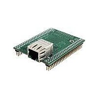
MOD5234-100IR
Manufacturer Part Number
MOD5234-100IR
Description
MOD5234 10/100 ETHERNET MODULE
Manufacturer
NetBurner Inc
Type
Controllers & Processorsr
Datasheets
1.MOD5272-100IR.pdf
(3 pages)
2.MOD5234-100IR.pdf
(4 pages)
3.MOD5234-100IR.pdf
(754 pages)
Specifications of MOD5234-100IR
Interface
I²C, SPI, UART
Voltage - Supply
2.5V
Mounting Type
Surface Mount
Package / Case
Module
Product
Modules
Lead Free Status / RoHS Status
Lead free / RoHS Compliant
Data Format
-
Baud Rates
-
Lead Free Status / Rohs Status
Lead free / RoHS Compliant
Other names
Q4483564


Freescale Semiconductor
11–10
Bits
7–6
5–1
9
8
0
C/I, SC, SD,
UC, UD
Name
PRI1
PRI0
SPV
WP
—
V
Table 6-1. RAMBAR Field Descriptions (Continued)
Priority bit. PRI1 determines if DMA/FEC or CPU has priority in upper 32k bank of memory.
PRI0 determines if DMA/FEC or CPU has priority in lower 32k bank of memory. If bit is set,
DMA/FEC has priority. If bit is cleared, CPU has priority. Priority is determined according
to the following table.
Note: The recommended setting for the priority bits is 00.
Secondary port valid. Allows access by DMA and FEC
0 DMA and FEC access to memory is disabled.
1 DMA and FEC access to memory is enabled.
Note: The BDE bit in the second RAMBAR register must also be set to allow dual port
access to the SRAM. For more information, see
Register (RAMBAR).”
Write protect. Allows only read accesses to the SRAM. When this bit is set, any attempted
write access will generate an access error exception to the ColdFire processor core.
0 Allows read and write accesses to the SRAM module
1 Allows only read accesses to the SRAM module
Reserved, should be cleared.
Address space masks (ASn)
These five bit fields allow certain types of accesses to be “masked,” or inhibited from
accessing the SRAM module. The address space mask bits are:
C/I = CPU space/interrupt acknowledge cycle mask
SC = Supervisor code address space mask
SD = Supervisor data address space mask
UC = User code address space mask
UD = User data address space mask
For each address space bit:
0 An access to the SRAM module can occur for this address space
1 Disable this address space from the SRAM module. If a reference using this address
These bits are useful for power management as detailed in
Management.”
Valid. A hardware reset clears this bit. When set, this bit enables the SRAM module;
otherwise, the module is disabled.
0 Contents of RAMBAR are not valid
1 Contents of RAMBAR are valid
space is made, it is inhibited from accessing the SRAM module, and is processed like
any other non-SRAM reference.
MCF5235 Reference Manual, Rev. 2
PRI[1:0]
00
01
10
11
Upper Bank Priority
DMA/FEC Accesses
DMA/FEC Accesses
CPU Accesses
CPU Accesses
Description
Section 11.2.1.2, “Memory Base Address
Lower Bank Priority
DMA/FEC Accesses
DMA/FEC Accesses
CPU Accesses
CPU Accesses
Section 6.2.4, “Power
Register Description
6-3
Related parts for MOD5234-100IR
Image
Part Number
Description
Manufacturer
Datasheet
Request
R

Part Number:
Description:
MCU, MPU & DSP Development Tools MOD5234 MODULE
Manufacturer:
NetBurner Inc
Datasheet:

Part Number:
Description:
MCU, MPU & DSP Development Tools MOD5234 Core Module Development Kit
Manufacturer:
NetBurner Inc
Datasheet:

Part Number:
Description:
BOARD SERIAL-ETHERNET 512K FLASH
Manufacturer:
NetBurner Inc
Datasheet:

Part Number:
Description:
PROCESSOR MODULE FLASH MOD5272
Manufacturer:
NetBurner Inc
Datasheet:

Part Number:
Description:
PROCESSOR MODULE 512KB FLASH
Manufacturer:
NetBurner Inc
Datasheet:

Part Number:
Description:
DUAL PORT SERIAL-ETHERNET
Manufacturer:
NetBurner Inc
Datasheet:

Part Number:
Description:
PROCESSOR MODULE FLASH
Manufacturer:
NetBurner Inc
Datasheet:

Part Number:
Description:
PROCESSOR MODULE 512KB FLASH
Manufacturer:
NetBurner Inc
Datasheet:

Part Number:
Description:
KIT DEVELOP NETWORK FOR MOD5282
Manufacturer:
NetBurner Inc
Datasheet:

Part Number:
Description:
KIT DEVELOP NETWORK FOR MOD5272
Manufacturer:
NetBurner Inc
Datasheet:

Part Number:
Description:
DUAL PORT SERIAL-ETHERNET
Manufacturer:
NetBurner Inc
Datasheet:

Part Number:
Description:
Ethernet Modules & Development Tools 32 Bit 66MHz 40 Pin DIP Industrial Temp
Manufacturer:
NetBurner Inc
Datasheet:

Part Number:
Description:
Ethernet ICs 32bit 147MHz CAN-to- Ethnt Device IndTemp
Manufacturer:
NetBurner Inc
Datasheet: