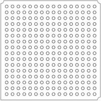
LFXP2-5E-5FTN256I Lattice, LFXP2-5E-5FTN256I Datasheet - Page 325

LFXP2-5E-5FTN256I
Manufacturer Part Number
LFXP2-5E-5FTN256I
Description
FPGA - Field Programmable Gate Array 5K LUTs 172 I/O Inst on DSP 1.2V -5 Spd
Manufacturer
Lattice
Datasheet
1.LFXP2-8E-5FTN256I.pdf
(341 pages)
Specifications of LFXP2-5E-5FTN256I
Number Of Macrocells
5000
Number Of Programmable I/os
172
Data Ram Size
169984
Supply Voltage (max)
1.26 V
Maximum Operating Temperature
+ 100 C
Minimum Operating Temperature
- 40 C
Mounting Style
SMD/SMT
Supply Voltage (min)
1.14 V
Package / Case
FTBGA-256
Number Of Logic Elements/cells
*
Number Of Labs/clbs
*
Total Ram Bits
169984
Number Of I /o
172
Number Of Gates
-
Voltage - Supply
1.14 V ~ 1.26 V
Mounting Type
*
Operating Temperature
-40°C ~ 100°C
Lead Free Status / RoHS Status
Lead free / RoHS Compliant
Available stocks
Company
Part Number
Manufacturer
Quantity
Price
Company:
Part Number:
LFXP2-5E-5FTN256I
Manufacturer:
Lattice
Quantity:
135
Company:
Part Number:
LFXP2-5E-5FTN256I
Manufacturer:
LATTICE
Quantity:
23
Company:
Part Number:
LFXP2-5E-5FTN256I
Manufacturer:
Lattice Semiconductor Corporation
Quantity:
10 000
Part Number:
LFXP2-5E-5FTN256I
Manufacturer:
LATTICE
Quantity:
20 000
- Current page: 325 of 341
- Download datasheet (10Mb)
Lattice Semiconductor
B. If the CFG1 pin is set to low (0), then the device will activate the Master SPI engine to boot the first pattern in. If
From the dual boot flow described above, it should become obvious why the Done fuse is always the very first fuse
to be erased when performing an erase operation. Also, it is the last Flash fuse to be programmed when
programming embedded Flash in LatticeXP2 devices.
Critical Points
failure occurs, as described above in 2a or 2b, the device will drive the INITN pin low and then high, and then
check if the Flash-Done fuse is programmed. If the Done fuse is programmed, the device will perform the SDM,
drive the DONE pin high, and the device wakes up. If the Done fuse is not programmed, then the device stops
configuring and leaves the DONE pin low to indicate configuration did not complete.
2. Done Fuse Not Programmed (aka Erased)
1. Check the maximum read frequency supported by the SPI Flash devices. Do not set the CCLK frequency
2. If the JTAG port has been used, do not toggle the PROGRAMN pin to reboot unless the board has been
tern. The device will boot from the embedded Flash. If it is desirable to check if the boot from the embed-
ded Flash is error free, the One Shot SED feature can be used to confirm.
Note: The devices carry out the one shot SED by reading the SRAM fuses and calculate the CRC value in
Background mode.
If the Done fuse is erased, then the embedded Flash must have an invalid pattern. The device will activate
the Master SPI engine to load the data from the external SPI Flash device. The standard protocol of the
Master SPI engine is to ignore the first 128 bits of data from the SPI Flash device, and then begins looking
for the preamble code 0xBDB3.
There are two possible failures.
in the bitstream beyond the maximum as specified on the data sheet of the SPI Flash devices.
Reason: All SPI Flash devices support Slow Read command (0x03) and Fast Read command (0x0B). The
LatticeXP2 family only supports the Slow Read command.
When the device is powered up, the CCLK frequency is the silicon default, which is approximately 3.1 MHz.
After the LatticeXP2 starts loading the bitstream, the CCLK frequency is updated to user’s selected fre-
quency. If the selected CCLK frequency exceeds maximum frequency supported by the SPI Flash device,
the LatticeXP2 may not configure.
Work-around Solution: When using the ispUFW to convert the JEDEC file into a bitstream file, select a
CCLK frequency setting that meets the specifications of the target SPI Flash.
power cycled. (Note 2 of the Signal Descriptions Table of DS1009,
Figure 18, describes this restriction.)
a. The preamble code is not detected within ~16K clocks. This will happen if the SPI Flash device is blank.
b. The CRC value calculated by the Master SPI engine of the device does not match with the one embed-
This is known as a time out failure.
ded in the bitstream. This means the bitstream is corrupted.
If there is a failure, the device drives the INITN pin low to indicate a failure. Otherwise, the device wakes
up and functions.
Note: The INITN pin is functional only when the Master SPI engine is active. Otherwise, it has no func-
tion.
17-7
LatticeXP2 Family Data
LatticeXP2 Dual Boot Feature
Sheet, shown in
Related parts for LFXP2-5E-5FTN256I
Image
Part Number
Description
Manufacturer
Datasheet
Request
R

Part Number:
Description:
FPGA - Field Programmable Gate Array 5K LUTs 146I/O Inst- on DSP 1.2V -5 Spd
Manufacturer:
Lattice
Datasheet:

Part Number:
Description:
FPGA - Field Programmable Gate Array 5K LUTs 172I/O Inst- on DSP 1.2V -5 Spd
Manufacturer:
Lattice
Datasheet:

Part Number:
Description:
FPGA - Field Programmable Gate Array 5K LUTs 100 I/O Inst on DSP 1.2V -5 Spd
Manufacturer:
Lattice
Datasheet:

Part Number:
Description:
FPGA - Field Programmable Gate Array 5K LUTs 100I/O Inst- on DSP 1.2V -5 Spd
Manufacturer:
Lattice
Datasheet:
Part Number:
Description:
FPGA LatticeXP2 Family 5000 Cells Flash Technology 1.2V 256-Pin FTBGA
Manufacturer:
LATTICE SEMICONDUCTOR
Datasheet:
Part Number:
Description:
FPGA LatticeXP2 Family 5000 Cells Flash Technology 1.2V 256-Pin FTBGA
Manufacturer:
LATTICE SEMICONDUCTOR
Datasheet:

Part Number:
Description:
IC DSP 5KLUTS 100I/O 144TQFP
Manufacturer:
Lattice
Datasheet:

Part Number:
Description:
IC DSP 5KLUTS 86I/O 132CSBGA
Manufacturer:
Lattice
Datasheet:

Part Number:
Description:
IC DSP 5KLUTS 86I/O 132CSBGA
Manufacturer:
Lattice
Datasheet:

Part Number:
Description:
IC DSP 5KLUTS 146I/O 208PQFP
Manufacturer:
Lattice
Datasheet:

Part Number:
Description:
IC DSP 5KLUTS 146I/O 208PQFP
Manufacturer:
Lattice
Datasheet:

Part Number:
Description:
IC DSP 5KLUTS 172I/O 256FTBGA
Manufacturer:
Lattice
Datasheet:

Part Number:
Description:
IC FPGA 5KLUTS 86I/O 132-BGA
Manufacturer:
Lattice
Datasheet:

Part Number:
Description:
IC FPGA 5KLUTS 86I/O 132-BGA
Manufacturer:
Lattice
Datasheet:

Part Number:
Description:
IC FPGA 5KLUTS 86I/O 132-BGA
Manufacturer:
Lattice
Datasheet:


