LFXP2-5E-5FTN256I Lattice, LFXP2-5E-5FTN256I Datasheet - Page 208

LFXP2-5E-5FTN256I
Manufacturer Part Number
LFXP2-5E-5FTN256I
Description
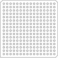
FPGA - Field Programmable Gate Array 5K LUTs 172 I/O Inst on DSP 1.2V -5 Spd
Manufacturer
Lattice
Datasheet
1.LFXP2-8E-5FTN256I.pdf
(341 pages)
Specifications of LFXP2-5E-5FTN256I
Number Of Macrocells
5000
Number Of Programmable I/os
172
Data Ram Size
169984
Supply Voltage (max)
1.26 V
Maximum Operating Temperature
+ 100 C
Minimum Operating Temperature
- 40 C
Mounting Style
SMD/SMT
Supply Voltage (min)
1.14 V
Package / Case
FTBGA-256
Number Of Logic Elements/cells
*
Number Of Labs/clbs
*
Total Ram Bits
169984
Number Of I /o
172
Number Of Gates
-
Voltage - Supply
1.14 V ~ 1.26 V
Mounting Type
*
Operating Temperature
-40°C ~ 100°C
Lead Free Status / RoHS Status
Lead free / RoHS Compliant
Available stocks
Company
Part Number
Manufacturer
Quantity
Price
Company:
Part Number:
LFXP2-5E-5FTN256I
Manufacturer:
Lattice
Quantity:
135
Company:
Part Number:
LFXP2-5E-5FTN256I
Manufacturer:
LATTICE
Quantity:
23
Company:
Part Number:
LFXP2-5E-5FTN256I
Manufacturer:
Lattice Semiconductor Corporation
Quantity:
10 000
Part Number:
LFXP2-5E-5FTN256I
Manufacturer:
LATTICE
Quantity:
20 000
- Current page: 208 of 341
- Download datasheet (10Mb)
Lattice Semiconductor
Figure 11-5 shows a typical DQ-DQS group for LatticeXP2 devices. The ninth I/O of this group of 16 or 18 I/Os is
the dedicated DQS pin. The 8 pads before of the DQS and 6/9 (6 for left and right side and 9 for top and bottom
side) pads after the DQS are covered by the DQS bus span. Users can assign any eight of these I/O pads to be DQ
data pins. Hence, to implement a 32-bit wide memory interface you would need to use four such DQ-DQS groups.
When not interfacing with the memory, the dedicated DQS pin can be used as a general purpose I/O. Each of the
dedicated DQS pin is internally connected to the DQS phase shift circuitry. The pinout information contained in the
LatticeXP2 Family Data Sheet
DDR Software Primitives
This section describes the software primitives that can be used to implement DDR interfaces. These primitives
include:
• DQSDLL – The DQS delay calibration DLL
• DQSBUFC – The DQS delay function and the clock polarity selection logic
• IDDRMX1A – The DDR input and DQS to system clock transfer registers with half clock cycle transfer
• IDDRMFX1A – The DDR input and DQS to system clock transfer registers with full clock cycle transfer
• ODDRMXA – The DDR output registers
HDL usage examples for each of these primitives are listed in Appendices A and B.
DQSDLL
The DQSDLL generates a 90-degree phase shift required for the DQS signal. This primitive implements the on-
chip DQSDLL. Only one DQSDLL should be instantiated for all the DDR implementations on one half of the device.
The clock input to this DLL should be at the same frequency as the DDR interface. The DLL generates the delay
based on this clock frequency and the update control input to this block. The DLL updates the dynamic delay con-
trol to the DQS delay block when this update control (UDDCNTL) input is asserted. Figure 11-6 shows the primitive
symbol. The active low signal on UDDCNTL updates the DQS phase alignment and should be initiated at the
beginning of READ cycles.
Figure 11-6. DQSDLL Symbol
Table 11-1 provides a description of the ports.
Table 11-1. DQSDLL Ports
DQSDLL Update Control: The DQS Delay can be updated for PVT variation using the UDDCNTL input. The
DQSDEL is updated when the when the UDDCNTL is held LOW. The DQSDEL can be updated when variations
are expected. DQSDEL can be updated anytime, except when the memory controller is receiving data from the
memory.
CLK
RST
UDDCNTL
LOCK
DQSDEL
Port Name
I/O
O
O
I
I
I
System CLK should be at the frequency of the DDR interface from the FPGA core.
Resets the DQSDLL
Provides update signal to the DLL that will update the dynamic delay.
Indicates when the DLL is in phase.
The digital delay generated by the DLL, should be connected to the DQSBUF primitive.
shows pin locations for the DQS pads.
CLK
RST
UDDCNTL
DQSDLL
11-4
DQSDEL
Description
LOCK
LatticeXP2 High-Speed I/O Interface
Related parts for LFXP2-5E-5FTN256I
Image
Part Number
Description
Manufacturer
Datasheet
Request
R

Part Number:
Description:
FPGA - Field Programmable Gate Array 5K LUTs 146I/O Inst- on DSP 1.2V -5 Spd
Manufacturer:
Lattice
Datasheet:

Part Number:
Description:
FPGA - Field Programmable Gate Array 5K LUTs 172I/O Inst- on DSP 1.2V -5 Spd
Manufacturer:
Lattice
Datasheet:

Part Number:
Description:
FPGA - Field Programmable Gate Array 5K LUTs 100 I/O Inst on DSP 1.2V -5 Spd
Manufacturer:
Lattice
Datasheet:

Part Number:
Description:
FPGA - Field Programmable Gate Array 5K LUTs 100I/O Inst- on DSP 1.2V -5 Spd
Manufacturer:
Lattice
Datasheet:
Part Number:
Description:
FPGA LatticeXP2 Family 5000 Cells Flash Technology 1.2V 256-Pin FTBGA
Manufacturer:
LATTICE SEMICONDUCTOR
Datasheet:
Part Number:
Description:
FPGA LatticeXP2 Family 5000 Cells Flash Technology 1.2V 256-Pin FTBGA
Manufacturer:
LATTICE SEMICONDUCTOR
Datasheet:

Part Number:
Description:
IC DSP 5KLUTS 100I/O 144TQFP
Manufacturer:
Lattice
Datasheet:

Part Number:
Description:
IC DSP 5KLUTS 86I/O 132CSBGA
Manufacturer:
Lattice
Datasheet:

Part Number:
Description:
IC DSP 5KLUTS 86I/O 132CSBGA
Manufacturer:
Lattice
Datasheet:

Part Number:
Description:
IC DSP 5KLUTS 146I/O 208PQFP
Manufacturer:
Lattice
Datasheet:

Part Number:
Description:
IC DSP 5KLUTS 146I/O 208PQFP
Manufacturer:
Lattice
Datasheet:

Part Number:
Description:
IC DSP 5KLUTS 172I/O 256FTBGA
Manufacturer:
Lattice
Datasheet:

Part Number:
Description:
IC FPGA 5KLUTS 86I/O 132-BGA
Manufacturer:
Lattice
Datasheet:

Part Number:
Description:
IC FPGA 5KLUTS 86I/O 132-BGA
Manufacturer:
Lattice
Datasheet:

Part Number:
Description:
IC FPGA 5KLUTS 86I/O 132-BGA
Manufacturer:
Lattice
Datasheet:


