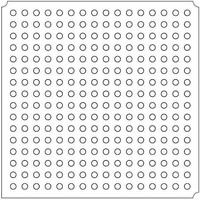
LFXP2-5E-5FTN256I Lattice, LFXP2-5E-5FTN256I Datasheet - Page 219

LFXP2-5E-5FTN256I
Manufacturer Part Number
LFXP2-5E-5FTN256I
Description
FPGA - Field Programmable Gate Array 5K LUTs 172 I/O Inst on DSP 1.2V -5 Spd
Manufacturer
Lattice
Datasheet
1.LFXP2-8E-5FTN256I.pdf
(341 pages)
Specifications of LFXP2-5E-5FTN256I
Number Of Macrocells
5000
Number Of Programmable I/os
172
Data Ram Size
169984
Supply Voltage (max)
1.26 V
Maximum Operating Temperature
+ 100 C
Minimum Operating Temperature
- 40 C
Mounting Style
SMD/SMT
Supply Voltage (min)
1.14 V
Package / Case
FTBGA-256
Number Of Logic Elements/cells
*
Number Of Labs/clbs
*
Total Ram Bits
169984
Number Of I /o
172
Number Of Gates
-
Voltage - Supply
1.14 V ~ 1.26 V
Mounting Type
*
Operating Temperature
-40°C ~ 100°C
Lead Free Status / RoHS Status
Lead free / RoHS Compliant
Available stocks
Company
Part Number
Manufacturer
Quantity
Price
Company:
Part Number:
LFXP2-5E-5FTN256I
Manufacturer:
Lattice
Quantity:
135
Company:
Part Number:
LFXP2-5E-5FTN256I
Manufacturer:
LATTICE
Quantity:
23
Company:
Part Number:
LFXP2-5E-5FTN256I
Manufacturer:
Lattice Semiconductor Corporation
Quantity:
10 000
Part Number:
LFXP2-5E-5FTN256I
Manufacturer:
LATTICE
Quantity:
20 000
- Current page: 219 of 341
- Download datasheet (10Mb)
Lattice Semiconductor
Data Valid Module
The data valid module generates a DATAVALID signal. This signal indicates to the FPGA that valid data is transmit-
ted out the input DDR registers to the FPGA core.
DDR I/O Register Implementation
The first set of DDR registers is used to de-mux the DDR data at the positive and negative edge of the phase
shifted DQS signal. The register that captures the positive-edge data is followed by a negative-edge triggered reg-
ister. This register transfers the positive edge data from the first register to the negative edge of DQS so that both
the positive and negative portions of the data are now aligned to the negative edge of DQS.
The second stage of registers is clocked by the FPGA clock, the polarity of this clock is selected by the DDR Clock
Polarity signal generated by the DQS Transition Detect Block.
The I/O Logic registers can be implemented in two modes:
• Half Clock Transfer Mode
• Full Clock Transfer Mode
In Half Clock Transfer mode the data is transferred to the FPGA core after the second stage of the register. In Full
Clock Transfer mode, an additional stage of I/O registers clocked by the FPGA clock is used to transfer the data to
the FPGA core.
The
Memory Read Implementation in Software
Three primitives in the ispLEVER
resents the DLL used for calibration. The IDDRMX1A/IDDRMFX1A primitive represents the DDR input registers
and clock domain transfer registers with or without full clock transfer. Finally, the DQSBUFC represents the DQS
delay block, the clock polarity control logic and the Data Valid module. Figures 11-19 and 11-20 show the READ
interface block generated using the IPexpress™ tool in the ispLEVER software.
Figure 11-19. Software Primitive Implementation for Memory READ (Half Clock Transfer)
dqs
dq
LatticeXP2 Family Data Sheet
uddcntl
reset
read
xclk
clk
ce
®
RST
UDDCNTL
DQSI
CLK
READ
XCLK
design tools represent the capability of these three elements. The DQSDLL rep-
explains each of these circuit elements in more detail.
DQSBUFC
DQSDEL
DQSDEL
DQSDLL
6
DDRCLKPOL
DATAVALID
PRMBDET
DQSXFER
11-15
DQSO
DQSC
LOCK
LatticeXP2 High-Speed I/O Interface
D
ECLK
DDRCLKPOL
RST
CE
SCLK
IDDRMX1A
QA
QB
datavalid
dqsc
prmbdet
dqsxfer
lock
datain_p
datain_n
Related parts for LFXP2-5E-5FTN256I
Image
Part Number
Description
Manufacturer
Datasheet
Request
R

Part Number:
Description:
FPGA - Field Programmable Gate Array 5K LUTs 146I/O Inst- on DSP 1.2V -5 Spd
Manufacturer:
Lattice
Datasheet:

Part Number:
Description:
FPGA - Field Programmable Gate Array 5K LUTs 172I/O Inst- on DSP 1.2V -5 Spd
Manufacturer:
Lattice
Datasheet:

Part Number:
Description:
FPGA - Field Programmable Gate Array 5K LUTs 100 I/O Inst on DSP 1.2V -5 Spd
Manufacturer:
Lattice
Datasheet:

Part Number:
Description:
FPGA - Field Programmable Gate Array 5K LUTs 100I/O Inst- on DSP 1.2V -5 Spd
Manufacturer:
Lattice
Datasheet:
Part Number:
Description:
FPGA LatticeXP2 Family 5000 Cells Flash Technology 1.2V 256-Pin FTBGA
Manufacturer:
LATTICE SEMICONDUCTOR
Datasheet:
Part Number:
Description:
FPGA LatticeXP2 Family 5000 Cells Flash Technology 1.2V 256-Pin FTBGA
Manufacturer:
LATTICE SEMICONDUCTOR
Datasheet:

Part Number:
Description:
IC DSP 5KLUTS 100I/O 144TQFP
Manufacturer:
Lattice
Datasheet:

Part Number:
Description:
IC DSP 5KLUTS 86I/O 132CSBGA
Manufacturer:
Lattice
Datasheet:

Part Number:
Description:
IC DSP 5KLUTS 86I/O 132CSBGA
Manufacturer:
Lattice
Datasheet:

Part Number:
Description:
IC DSP 5KLUTS 146I/O 208PQFP
Manufacturer:
Lattice
Datasheet:

Part Number:
Description:
IC DSP 5KLUTS 146I/O 208PQFP
Manufacturer:
Lattice
Datasheet:

Part Number:
Description:
IC DSP 5KLUTS 172I/O 256FTBGA
Manufacturer:
Lattice
Datasheet:

Part Number:
Description:
IC FPGA 5KLUTS 86I/O 132-BGA
Manufacturer:
Lattice
Datasheet:

Part Number:
Description:
IC FPGA 5KLUTS 86I/O 132-BGA
Manufacturer:
Lattice
Datasheet:

Part Number:
Description:
IC FPGA 5KLUTS 86I/O 132-BGA
Manufacturer:
Lattice
Datasheet:


