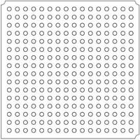
LFXP2-5E-5FTN256I Lattice, LFXP2-5E-5FTN256I Datasheet - Page 243

LFXP2-5E-5FTN256I
Manufacturer Part Number
LFXP2-5E-5FTN256I
Description
FPGA - Field Programmable Gate Array 5K LUTs 172 I/O Inst on DSP 1.2V -5 Spd
Manufacturer
Lattice
Datasheet
1.LFXP2-8E-5FTN256I.pdf
(341 pages)
Specifications of LFXP2-5E-5FTN256I
Number Of Macrocells
5000
Number Of Programmable I/os
172
Data Ram Size
169984
Supply Voltage (max)
1.26 V
Maximum Operating Temperature
+ 100 C
Minimum Operating Temperature
- 40 C
Mounting Style
SMD/SMT
Supply Voltage (min)
1.14 V
Package / Case
FTBGA-256
Number Of Logic Elements/cells
*
Number Of Labs/clbs
*
Total Ram Bits
169984
Number Of I /o
172
Number Of Gates
-
Voltage - Supply
1.14 V ~ 1.26 V
Mounting Type
*
Operating Temperature
-40°C ~ 100°C
Lead Free Status / RoHS Status
Lead free / RoHS Compliant
Available stocks
Company
Part Number
Manufacturer
Quantity
Price
Company:
Part Number:
LFXP2-5E-5FTN256I
Manufacturer:
Lattice
Quantity:
135
Company:
Part Number:
LFXP2-5E-5FTN256I
Manufacturer:
LATTICE
Quantity:
23
Company:
Part Number:
LFXP2-5E-5FTN256I
Manufacturer:
Lattice Semiconductor Corporation
Quantity:
10 000
Part Number:
LFXP2-5E-5FTN256I
Manufacturer:
LATTICE
Quantity:
20 000
- Current page: 243 of 341
- Download datasheet (10Mb)
Lattice Semiconductor
Table 11-14. User Parameters in the IPexpress GUI when in DDR2 Mode
FCRAM (“Fast Cycle Random Access Memory”) Interface
FCRAM is a DDR-type DRAM, which performs data output at both the rising and falling edges of the clock. FCRAM
devices operate at a core voltage of 2.5V with SSTL Class II I/O. It has enhanced both the core and peripheral logic
of the SDRAM. In FCRAM the address and command signals are synchronized with the clock input, and the data
pins are synchronized with the DQS signal. Data output takes place at both the rising and falling edges of the DQS.
DQS is in phase with the clock input of the device. The DDR SDRAM and DDR FCRAM controller will have differ-
ent pinouts.
LatticeXP2 devices can implement the FCRAM interface using dedicated DQS logic, input DDR registers and out-
put DDR registers, as described in the Implementing Memory Interfaces section of this document. Generation of
address and control signals for FCRAM are different than in DDR SDRAM devices. Please refer to the FCRAM
data sheets to see detailed specifications. Toshiba, Inc. and Fujitsu, Inc. offer FCRAM devices in 256Mb densities.
They are available in x8 or x16 configurations.
Board Design Guidelines
The most common challenge associated with implementing DDR memory interfaces is the board design and lay-
out. It is required that users strictly follow the guidelines recommended by memory device vendors.
Some of the common recommendations include matching trace lengths of interface signals to avoid skew, proper
DQ-DQS signal grouping, proper termination of the SSTL2 or SSTL18 I/O Standard, proper VREF and VTT gener-
ation decoupling and proper PCB routing.
The following documents include board layout guidelines:
• www.idt.com, IDT, PCB Design for Double Data Rate Memory
• www.motorola.com, AN2582, Hardware and Layout Design Considerations for DDR Interfaces
References
• www.jedec.org, JEDEC Standard 79, Double Data Rate (DDR) SDRAM Specification
• www.micron.com, DDR SDRAM Data Sheets
I/O Buffer Configuration
Data Width
Number of DQS
Frequency of DQS
Lock/Jitter Sensitivity
LSR for DDR Input Register
Create Clock Enable for DDR
Input Register
Tri-state Enable for DDR
Output Registers
DDR Tristate enable for the
DQS output
DQS Buffer Configuration for
DDR2
User Parameters
LSR Control
I/O Standard used for the Interface. This will
also depend on the Mode selected.
Width of the Data bus
Number of DQS will determine the number of
DQS Groups
DDR Interface Frequency. This is also input to
the DDR DLL. The values will depend on the
mode selected.
DLL Sensitivity to Jitter
Create Clock enable inputs to the block
Creates Tri-state control for the DDR data output
registers.
Creates Tristate control for DQS output
DQS Buffer can be configured as Differential
Description
11-39
LatticeXP2 High-Speed I/O Interface
166MHz, 200MHz, 266MHz
SSTL18_I, SSTL18_II
Values/Range
RESET, SET
High, Low
1, 2, 4, 8
On/Off
On/Off
On/Off
On/Off
8-64
SSTL18_I
200MHz
Default
RESET
High
Off
On
On
Off
8
1
Related parts for LFXP2-5E-5FTN256I
Image
Part Number
Description
Manufacturer
Datasheet
Request
R

Part Number:
Description:
FPGA - Field Programmable Gate Array 5K LUTs 146I/O Inst- on DSP 1.2V -5 Spd
Manufacturer:
Lattice
Datasheet:

Part Number:
Description:
FPGA - Field Programmable Gate Array 5K LUTs 172I/O Inst- on DSP 1.2V -5 Spd
Manufacturer:
Lattice
Datasheet:

Part Number:
Description:
FPGA - Field Programmable Gate Array 5K LUTs 100 I/O Inst on DSP 1.2V -5 Spd
Manufacturer:
Lattice
Datasheet:

Part Number:
Description:
FPGA - Field Programmable Gate Array 5K LUTs 100I/O Inst- on DSP 1.2V -5 Spd
Manufacturer:
Lattice
Datasheet:
Part Number:
Description:
FPGA LatticeXP2 Family 5000 Cells Flash Technology 1.2V 256-Pin FTBGA
Manufacturer:
LATTICE SEMICONDUCTOR
Datasheet:
Part Number:
Description:
FPGA LatticeXP2 Family 5000 Cells Flash Technology 1.2V 256-Pin FTBGA
Manufacturer:
LATTICE SEMICONDUCTOR
Datasheet:

Part Number:
Description:
IC DSP 5KLUTS 100I/O 144TQFP
Manufacturer:
Lattice
Datasheet:

Part Number:
Description:
IC DSP 5KLUTS 86I/O 132CSBGA
Manufacturer:
Lattice
Datasheet:

Part Number:
Description:
IC DSP 5KLUTS 86I/O 132CSBGA
Manufacturer:
Lattice
Datasheet:

Part Number:
Description:
IC DSP 5KLUTS 146I/O 208PQFP
Manufacturer:
Lattice
Datasheet:

Part Number:
Description:
IC DSP 5KLUTS 146I/O 208PQFP
Manufacturer:
Lattice
Datasheet:

Part Number:
Description:
IC DSP 5KLUTS 172I/O 256FTBGA
Manufacturer:
Lattice
Datasheet:

Part Number:
Description:
IC FPGA 5KLUTS 86I/O 132-BGA
Manufacturer:
Lattice
Datasheet:

Part Number:
Description:
IC FPGA 5KLUTS 86I/O 132-BGA
Manufacturer:
Lattice
Datasheet:

Part Number:
Description:
IC FPGA 5KLUTS 86I/O 132-BGA
Manufacturer:
Lattice
Datasheet:


