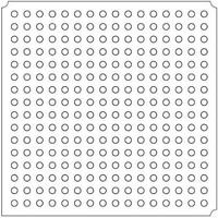
LFXP2-5E-5FTN256I Lattice, LFXP2-5E-5FTN256I Datasheet - Page 157

LFXP2-5E-5FTN256I
Manufacturer Part Number
LFXP2-5E-5FTN256I
Description
FPGA - Field Programmable Gate Array 5K LUTs 172 I/O Inst on DSP 1.2V -5 Spd
Manufacturer
Lattice
Datasheet
1.LFXP2-8E-5FTN256I.pdf
(341 pages)
Specifications of LFXP2-5E-5FTN256I
Number Of Macrocells
5000
Number Of Programmable I/os
172
Data Ram Size
169984
Supply Voltage (max)
1.26 V
Maximum Operating Temperature
+ 100 C
Minimum Operating Temperature
- 40 C
Mounting Style
SMD/SMT
Supply Voltage (min)
1.14 V
Package / Case
FTBGA-256
Number Of Logic Elements/cells
*
Number Of Labs/clbs
*
Total Ram Bits
169984
Number Of I /o
172
Number Of Gates
-
Voltage - Supply
1.14 V ~ 1.26 V
Mounting Type
*
Operating Temperature
-40°C ~ 100°C
Lead Free Status / RoHS Status
Lead free / RoHS Compliant
Available stocks
Company
Part Number
Manufacturer
Quantity
Price
Company:
Part Number:
LFXP2-5E-5FTN256I
Manufacturer:
Lattice
Quantity:
135
Company:
Part Number:
LFXP2-5E-5FTN256I
Manufacturer:
LATTICE
Quantity:
23
Company:
Part Number:
LFXP2-5E-5FTN256I
Manufacturer:
Lattice Semiconductor Corporation
Quantity:
10 000
Part Number:
LFXP2-5E-5FTN256I
Manufacturer:
LATTICE
Quantity:
20 000
- Current page: 157 of 341
- Download datasheet (10Mb)
Lattice Semiconductor
Table 10-2. EBR-based Single Port Memory Port Definitions
Reset (or RST) resets only the input and output registers of the RAM. It does not reset the contents of the memory.
Chip Select (CS) is a useful port in the EBR primitive when multiple cascaded EBR blocks are required by the
memory. The CS signal forms the MSB for the address when multiple EBR blocks are cascaded. CS is a 3-bit bus,
so it can cascade eight memories easily. If the memory size specified by the user requires more than eight EBR
blocks, the ispLEVER software automatically generates the additional address decoding logic, which is imple-
mented in the PFU (external to the EBR blocks).
Each EBR block consists of 18,432 bits of RAM. The values for x (address) and y (data) for each EBR block for the
devices are listed in Table 10-3.
Table 10-3. Single Port Memory Sizes for 16K Memories for LatticeXP2
Table 10-4 shows the various attributes available for the Single Port Memory (RAM_DQ). Some of these attributes
are user-selectable through the IPexpress GUI. For detailed attribute definitions, refer to Appendix A.
Generated Module
Port Name in
Memory Size
Single Port
512 x 36
ClockEn
Address
16K x 1
1K x 18
8K x 2
4K x 4
2K x 9
Reset
Clock
Data
WE
—
Q
EBR Block Primitive
Port Name in the
Input Data
DI[17:0]
DI[35:0]
DO[y:0]
CS[2:0]
AD[x:0]
DI[1:0]
DI[3:0]
DI[8:0]
DI[y:0]
CLK
RST
WE
CE
DI
10-7
Clock Enable
Address Bus
Write Enable
Output Data
Description
Chip Select
Data Out
DO[17:0]
DO[35:0]
DO[1:0]
DO[3:0]
DO[8:0]
Data In
Reset
Clock
DO
LatticeXP2 Memory Usage Guide
Address [MSB:LSB]
Rising Clock Edge
Active State
Active High
Active High
Active High
AD[12:0]
AD[11:0]
AD[10:0]
AD[13:0]
AD[9:0]
AD[8:0]
—
—
—
—
Related parts for LFXP2-5E-5FTN256I
Image
Part Number
Description
Manufacturer
Datasheet
Request
R

Part Number:
Description:
FPGA - Field Programmable Gate Array 5K LUTs 146I/O Inst- on DSP 1.2V -5 Spd
Manufacturer:
Lattice
Datasheet:

Part Number:
Description:
FPGA - Field Programmable Gate Array 5K LUTs 172I/O Inst- on DSP 1.2V -5 Spd
Manufacturer:
Lattice
Datasheet:

Part Number:
Description:
FPGA - Field Programmable Gate Array 5K LUTs 100 I/O Inst on DSP 1.2V -5 Spd
Manufacturer:
Lattice
Datasheet:

Part Number:
Description:
FPGA - Field Programmable Gate Array 5K LUTs 100I/O Inst- on DSP 1.2V -5 Spd
Manufacturer:
Lattice
Datasheet:
Part Number:
Description:
FPGA LatticeXP2 Family 5000 Cells Flash Technology 1.2V 256-Pin FTBGA
Manufacturer:
LATTICE SEMICONDUCTOR
Datasheet:
Part Number:
Description:
FPGA LatticeXP2 Family 5000 Cells Flash Technology 1.2V 256-Pin FTBGA
Manufacturer:
LATTICE SEMICONDUCTOR
Datasheet:

Part Number:
Description:
IC DSP 5KLUTS 100I/O 144TQFP
Manufacturer:
Lattice
Datasheet:

Part Number:
Description:
IC DSP 5KLUTS 86I/O 132CSBGA
Manufacturer:
Lattice
Datasheet:

Part Number:
Description:
IC DSP 5KLUTS 86I/O 132CSBGA
Manufacturer:
Lattice
Datasheet:

Part Number:
Description:
IC DSP 5KLUTS 146I/O 208PQFP
Manufacturer:
Lattice
Datasheet:

Part Number:
Description:
IC DSP 5KLUTS 146I/O 208PQFP
Manufacturer:
Lattice
Datasheet:

Part Number:
Description:
IC DSP 5KLUTS 172I/O 256FTBGA
Manufacturer:
Lattice
Datasheet:

Part Number:
Description:
IC FPGA 5KLUTS 86I/O 132-BGA
Manufacturer:
Lattice
Datasheet:

Part Number:
Description:
IC FPGA 5KLUTS 86I/O 132-BGA
Manufacturer:
Lattice
Datasheet:

Part Number:
Description:
IC FPGA 5KLUTS 86I/O 132-BGA
Manufacturer:
Lattice
Datasheet:


