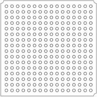
LFXP2-5E-5FTN256I Lattice, LFXP2-5E-5FTN256I Datasheet - Page 148

LFXP2-5E-5FTN256I
Manufacturer Part Number
LFXP2-5E-5FTN256I
Description
FPGA - Field Programmable Gate Array 5K LUTs 172 I/O Inst on DSP 1.2V -5 Spd
Manufacturer
Lattice
Datasheet
1.LFXP2-8E-5FTN256I.pdf
(341 pages)
Specifications of LFXP2-5E-5FTN256I
Number Of Macrocells
5000
Number Of Programmable I/os
172
Data Ram Size
169984
Supply Voltage (max)
1.26 V
Maximum Operating Temperature
+ 100 C
Minimum Operating Temperature
- 40 C
Mounting Style
SMD/SMT
Supply Voltage (min)
1.14 V
Package / Case
FTBGA-256
Number Of Logic Elements/cells
*
Number Of Labs/clbs
*
Total Ram Bits
169984
Number Of I /o
172
Number Of Gates
-
Voltage - Supply
1.14 V ~ 1.26 V
Mounting Type
*
Operating Temperature
-40°C ~ 100°C
Lead Free Status / RoHS Status
Lead free / RoHS Compliant
Available stocks
Company
Part Number
Manufacturer
Quantity
Price
Company:
Part Number:
LFXP2-5E-5FTN256I
Manufacturer:
Lattice
Quantity:
135
Company:
Part Number:
LFXP2-5E-5FTN256I
Manufacturer:
LATTICE
Quantity:
23
Company:
Part Number:
LFXP2-5E-5FTN256I
Manufacturer:
Lattice Semiconductor Corporation
Quantity:
10 000
Part Number:
LFXP2-5E-5FTN256I
Manufacturer:
LATTICE
Quantity:
20 000
- Current page: 148 of 341
- Download datasheet (10Mb)
Lattice Semiconductor
Appendix C. Clock Preferences
A few key clock preferences are introduced below. Refer to the ‘Help’ file for other preferences and detailed infor-
mation.
ASIC
The following preference command assigns a phase of 90 degrees to the CIMDLLA CLKOP.
FREQUENCY
The following physical preference command assigns a frequency of 100 MHz to a net named clk1:
The following preference specifies a hold margin value for each clock domain:
MAXSKEW
The following command assigns a maximum skew of 5 nanoseconds to a net named NetB:
MULTICYCLE
The following command will relax the period to 50 nanoseconds for the path starting at COMPA to COMPB (NET1):
PERIOD
The following command assigns a clock period of 30 nanoseconds to the port named Clk1:
PROHIBIT
This command prohibits the use of a primary clock to route a clock net named bf_clk:
USE PRIMARY
Use a primary clock resource to route the specified net:
USE SECONDARY
Use a secondary clock resource to route the specified net:
ASIC “my_dll” TYPE “CIMDLLA” CLKOP_PHASE=90;
FREQUENCY NET “clk1” 100 MHz;
FREQUENCY NET “RX_CLKA_CMOS_c” 100.000 MHz HOLD_MARGIN 1 ns;
MAXSKEW NET “NetB” 5 NS;
MULTICYCLE “PATH1” START COMP “COMPA” END COMP “COMPB” NET “NET1” 50 NS ;
PERIOD PORT “Clk1” 30 NS;
PROHIBIT PRIMARY NET “bf_clk”;
USE PRIMARY NET clk_fast;
USE PRIMARY DCS NET “bf_clk”;
USE PRIMARY PURE NET “bf_clk” QUADRANT_TL;
USE SECONDARY NET “clk_lessfast” QUADRANT_TL;
9-26
LatticeXP2 sysCLOCK PLL
Design and Usage Guide
Related parts for LFXP2-5E-5FTN256I
Image
Part Number
Description
Manufacturer
Datasheet
Request
R

Part Number:
Description:
FPGA - Field Programmable Gate Array 5K LUTs 146I/O Inst- on DSP 1.2V -5 Spd
Manufacturer:
Lattice
Datasheet:

Part Number:
Description:
FPGA - Field Programmable Gate Array 5K LUTs 172I/O Inst- on DSP 1.2V -5 Spd
Manufacturer:
Lattice
Datasheet:

Part Number:
Description:
FPGA - Field Programmable Gate Array 5K LUTs 100 I/O Inst on DSP 1.2V -5 Spd
Manufacturer:
Lattice
Datasheet:

Part Number:
Description:
FPGA - Field Programmable Gate Array 5K LUTs 100I/O Inst- on DSP 1.2V -5 Spd
Manufacturer:
Lattice
Datasheet:
Part Number:
Description:
FPGA LatticeXP2 Family 5000 Cells Flash Technology 1.2V 256-Pin FTBGA
Manufacturer:
LATTICE SEMICONDUCTOR
Datasheet:
Part Number:
Description:
FPGA LatticeXP2 Family 5000 Cells Flash Technology 1.2V 256-Pin FTBGA
Manufacturer:
LATTICE SEMICONDUCTOR
Datasheet:

Part Number:
Description:
IC DSP 5KLUTS 100I/O 144TQFP
Manufacturer:
Lattice
Datasheet:

Part Number:
Description:
IC DSP 5KLUTS 86I/O 132CSBGA
Manufacturer:
Lattice
Datasheet:

Part Number:
Description:
IC DSP 5KLUTS 86I/O 132CSBGA
Manufacturer:
Lattice
Datasheet:

Part Number:
Description:
IC DSP 5KLUTS 146I/O 208PQFP
Manufacturer:
Lattice
Datasheet:

Part Number:
Description:
IC DSP 5KLUTS 146I/O 208PQFP
Manufacturer:
Lattice
Datasheet:

Part Number:
Description:
IC DSP 5KLUTS 172I/O 256FTBGA
Manufacturer:
Lattice
Datasheet:

Part Number:
Description:
IC FPGA 5KLUTS 86I/O 132-BGA
Manufacturer:
Lattice
Datasheet:

Part Number:
Description:
IC FPGA 5KLUTS 86I/O 132-BGA
Manufacturer:
Lattice
Datasheet:

Part Number:
Description:
IC FPGA 5KLUTS 86I/O 132-BGA
Manufacturer:
Lattice
Datasheet:


