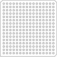
LFXP2-5E-5FTN256I Lattice, LFXP2-5E-5FTN256I Datasheet - Page 196

LFXP2-5E-5FTN256I
Manufacturer Part Number
LFXP2-5E-5FTN256I
Description
FPGA - Field Programmable Gate Array 5K LUTs 172 I/O Inst on DSP 1.2V -5 Spd
Manufacturer
Lattice
Datasheet
1.LFXP2-8E-5FTN256I.pdf
(341 pages)
Specifications of LFXP2-5E-5FTN256I
Number Of Macrocells
5000
Number Of Programmable I/os
172
Data Ram Size
169984
Supply Voltage (max)
1.26 V
Maximum Operating Temperature
+ 100 C
Minimum Operating Temperature
- 40 C
Mounting Style
SMD/SMT
Supply Voltage (min)
1.14 V
Package / Case
FTBGA-256
Number Of Logic Elements/cells
*
Number Of Labs/clbs
*
Total Ram Bits
169984
Number Of I /o
172
Number Of Gates
-
Voltage - Supply
1.14 V ~ 1.26 V
Mounting Type
*
Operating Temperature
-40°C ~ 100°C
Lead Free Status / RoHS Status
Lead free / RoHS Compliant
Available stocks
Company
Part Number
Manufacturer
Quantity
Price
Company:
Part Number:
LFXP2-5E-5FTN256I
Manufacturer:
Lattice
Quantity:
135
Company:
Part Number:
LFXP2-5E-5FTN256I
Manufacturer:
LATTICE
Quantity:
23
Company:
Part Number:
LFXP2-5E-5FTN256I
Manufacturer:
Lattice Semiconductor Corporation
Quantity:
10 000
Part Number:
LFXP2-5E-5FTN256I
Manufacturer:
LATTICE
Quantity:
20 000
- Current page: 196 of 341
- Download datasheet (10Mb)
Lattice Semiconductor
Figure 10-52. WRITE_DIS Waveform
ERASE_TAG (0Eh)
The ERASE_TAG command is enabled after the command WRITE_EN has been shifted into the device and exe-
cuted. The ERASE_TAG command erases all the TAG Memory Flash cells.
The command is executed when the Chip Select pin is driven from low to high after the 24th dummy clock. Any
extra dummy clocks, if presented before driving the Chip Select pin to high, are ignored. After the Chip Select pin is
driven from low to high, a minimum of three clocks is required to initiate the erase action. After the three clocks,
extra clocks are optional. Once the erase action is initiated, it will be carried out until it is done. There is no mecha-
nism to terminate the erase action.
This command sets the STATUS bit to 0 when the erase action begins. The programming engine sets the status bit
to 1 when the erase is done successfully.
Figure 10-53. ERASE_TAG Waveform
PROGRAM_TAG (8Eh)
The PROGRAM_TAG is enabled after the command WRITE_EN has been shifted into the device and executed.
The PROGRAM_TAG command programs the entire TAG memory page at once.
After the command is shifted into the device on the SI pin, and followed by 24 dummy clocks, the TAG memory col-
umn decoder serves as the data buffer for the programming data to be shifted into serially. The shifting direction is
from left to right, as shown. The first bit to be shifted out closest to the SO pin appears on the right-most side of the
shift register. The data buffer functions like a FIFO (First In First Out) serial data shift register. In order to make sure
that bit 0 will be read out first, data bit 0 must be shifted into the right-most location of the data shift register. To
achieve this, the data buffer must be filled up completely. Consequently, over-filling the data buffer will cause over-
flow of the data buffer, resulting in loss of data.
CS
CLK
SI
SO
CS
CLK
SI
SO
Shifting Clocks
Shifting Clocks
8 Command
8 Command
Three Clocks To Initiate the Erase Action
Three Clocks to Initiate And Complete
Optional Extra Clocks
Optional Extra Clocks
10-46
HIGH IMPEDANCE
HIGH IMPEDANCE
LatticeXP2 Memory Usage Guide
Related parts for LFXP2-5E-5FTN256I
Image
Part Number
Description
Manufacturer
Datasheet
Request
R

Part Number:
Description:
FPGA - Field Programmable Gate Array 5K LUTs 146I/O Inst- on DSP 1.2V -5 Spd
Manufacturer:
Lattice
Datasheet:

Part Number:
Description:
FPGA - Field Programmable Gate Array 5K LUTs 172I/O Inst- on DSP 1.2V -5 Spd
Manufacturer:
Lattice
Datasheet:

Part Number:
Description:
FPGA - Field Programmable Gate Array 5K LUTs 100 I/O Inst on DSP 1.2V -5 Spd
Manufacturer:
Lattice
Datasheet:

Part Number:
Description:
FPGA - Field Programmable Gate Array 5K LUTs 100I/O Inst- on DSP 1.2V -5 Spd
Manufacturer:
Lattice
Datasheet:
Part Number:
Description:
FPGA LatticeXP2 Family 5000 Cells Flash Technology 1.2V 256-Pin FTBGA
Manufacturer:
LATTICE SEMICONDUCTOR
Datasheet:
Part Number:
Description:
FPGA LatticeXP2 Family 5000 Cells Flash Technology 1.2V 256-Pin FTBGA
Manufacturer:
LATTICE SEMICONDUCTOR
Datasheet:

Part Number:
Description:
IC DSP 5KLUTS 100I/O 144TQFP
Manufacturer:
Lattice
Datasheet:

Part Number:
Description:
IC DSP 5KLUTS 86I/O 132CSBGA
Manufacturer:
Lattice
Datasheet:

Part Number:
Description:
IC DSP 5KLUTS 86I/O 132CSBGA
Manufacturer:
Lattice
Datasheet:

Part Number:
Description:
IC DSP 5KLUTS 146I/O 208PQFP
Manufacturer:
Lattice
Datasheet:

Part Number:
Description:
IC DSP 5KLUTS 146I/O 208PQFP
Manufacturer:
Lattice
Datasheet:

Part Number:
Description:
IC DSP 5KLUTS 172I/O 256FTBGA
Manufacturer:
Lattice
Datasheet:

Part Number:
Description:
IC FPGA 5KLUTS 86I/O 132-BGA
Manufacturer:
Lattice
Datasheet:

Part Number:
Description:
IC FPGA 5KLUTS 86I/O 132-BGA
Manufacturer:
Lattice
Datasheet:

Part Number:
Description:
IC FPGA 5KLUTS 86I/O 132-BGA
Manufacturer:
Lattice
Datasheet:


